ENGR 337
Lab 2020 Spring
Lab 09
Nic Theobald
nstheobald@fortlewis.edu
Electric VLSI Tutorial 4
Introduction
This Lab
covers the design of an ESD protection circuit and the inclusion of the circuit
into the input/output pads of the chip. ESD protection circuits are important
for preventing damage to the chip in the event of static shock. The next lab
will include the integration of this pad-ESD circuit into the actual inverter
chip.
Materials
|
Computer |
1 |
|
LTSPICE |
1 |
|
Electric VLSI |
1 |
|
Your Brain |
1 |
|
Some Patience |
1 |
Abbreviated
Methods
This lab
started off with the design of the ESD protection circuit. An n-act component (50x50)
was added to the layout with a metal 1 lead coming off of the top of the
component. A ring of p-well components was added with the given dimensions
(Figure 1). The same process was followed but for p-act and n-well components
(Figure 2). Both diode were then incorporated into the
pad circuit (Figure 3). The pad and ESD circuit is then arranged on a 5000x5000
frame and are all connected together with 84 width metal 3 wires (Figure 4).
Results
Design of
the ESD Protection Circuit
|
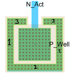
Figure
1: Nact Pwell Diode 1: (10x80) 2: (68x10) 3:
(30x10) |
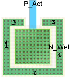
Figure
2: Pact Nwell
Diode 1:
(10x80) 2:
(68x10) 3:
(30x10) |
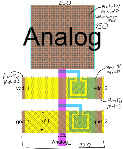
Figure
3: ESD Pad Circuit |
Padframe
and ESD Circuit
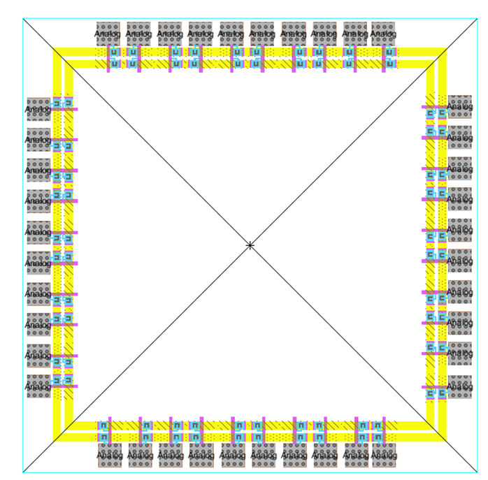
Figure 4: Pad Frame and ESD circuit
Discussion:
Several
problems were encountered in this lab. The pad frame never passed the DRC check
even though all wires were perfectly aligned. Simulation of the ESD was
attempted but never resulted in success. Further testing with components may
bring insight into what combinations cause error. The next step in the process
is to add the inverter circuit.