ENGR 337
Lab 2020 Spring
Lab 08
Nic Theobald
nstheobald@fortlewis.edu
Electric VLSI Tutorial 3
Introduction
This Lab covers the design of a inverter using P and N type MOSFETs. The input signal is applied to the gates of the transistors and an inverted signal is outputted through the drain of both transistors. The source of the PMOS is shorted to high and the source of the NMOS is shorted to low. When the input voltage is high, the NMOS pulls the output to low; and when the input is low, the PMOS pulls the output to high.
Materials
|
Computer |
1 |
|
LTSPICE |
1 |
|
Electric VLSI |
1 |
|
Your Brain |
1 |
|
Some Patience |
1 |
Abbreviated Methods
Both transistors were added to the schematic in the three-terminal configuration. The PMOS and NMOS were set up in traditional method except that an input was shorted to the gate of both transistors and an output to the drain of both transistors. Using this same idea, the transistors were built in the layout view using n-type and p-type substrates and “acts.”
Results
Design of the inverter using ElectricVLSI.
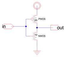
Figure 1: Inverter Schematic
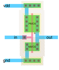
Figure 2: Inverter Layout
Inverter input and output simulation using LTspice.
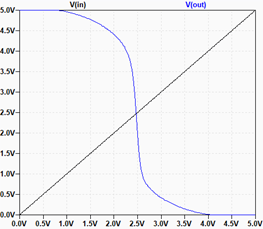
Figure 4: LTSPICE output
Discussion:
Electric VLSI was used to design and simulate an inverter base on PMOS and NMOS transistors. Electric VLSI proved especially useful in its ability to recognize mistakes in the design. Several techniques were used to recognize mistakes. Built in error checking tools were used to find mistakes in the schematic and layout. LTSPICE was used to make sure the circuit performed as expected. However, an unknown error occurred in the design of my inverter so Professor Li sent me his file.