ENGR 337
Lab 2020 Spring
Lab 07
Nic Theobald
nstheobald@fortlewis.edu
Electric VLSI Tutorial 2
Introduction
This Lab covers the operation of the VLSI software and the design of p-type and n-type MOSFETs. The ability to design MOSFETs with specific properties is useful when you want to minimize space or optimize the device for high current applications.
Materials
|
Computer |
1 |
|
LTSPICE |
1 |
|
Electric VLSI |
1 |
|
Your Brain |
1 |
|
Some Patience |
1 |
Abbreviated Methods
Tutorial 2 followed similar procedures as tutorial 1. Tutorial 2 follows the design of a P and N type MOSFET. Tutorial 1, like Tutorial 2, started with the creation of a new library, schematic, and layout. P-sub, n-well, and metal contacts were used to design the PMOS and NMOS transistors.
Results
Current simulation for the NMOS transistor.
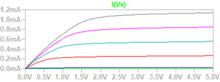
Figure 1: LTSPICE output NMOS
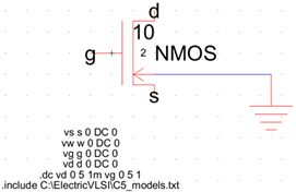
Figure 2: Electric VLSI Schematic NMOS
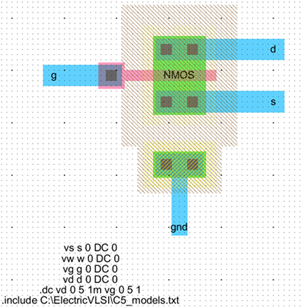
Figure 3: Electric VLSI Layout NMOS
Current simulation for the PMOS transistor.
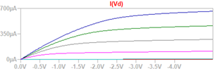
Figure 4: LTSPICE output PMOS
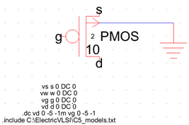
Figure 5: Electric VLSI Schematic PMOS
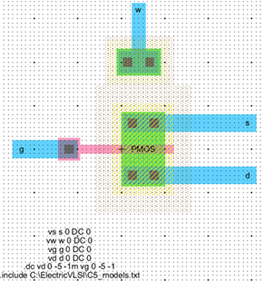
Figure 6: Electric VLSI Layout PMOS
Discussion:
Electric VLSI was used to design and simulate a PMOS and NMOS transistors. Electric VLSI proved especially useful in its ability to recognize mistakes in the design. Several techniques were used to recognize mistakes. Built in error checking tools were used to find mistakes in the schematic and layout. LTSPICE was used to make sure the circuit performed as expected.