ENGR 337 Lab 2020 Spring
Lab Final
Nic Theobald
nstheobald@fortlewis.edu
Electric VLSI Final Project
Introduction
This Lab covers the design of an OPAMP integrated circuit. The OPAMP includes the previously designed inverter and ESD Pad Frame. Pad Frame DRC errors reported in the last lab were resolved but resulted in the occurrence of a NCC error in the ESD Pad layout and schematic.
Materials
|
Materials |
|
|
Computer |
1 |
|
LTSPICE |
1 |
|
Electric VLSI |
1 |
|
Your Brain |
1 |
|
Some Patience |
1 |
Abbreviated Methods
This Lab covers the design an OPAMP integrated circuit. The first step was to design the inverter (Figure 1,2). The input signal is applied to the gates of the transistors and an inverted signal is outputted through the drain of both transistors. The source of the PMOS is shorted to high and the source of the NMOS is shorted to low. When the input voltage is high, the NMOS pulls the output to low; and when the input is low, the PMOS pulls the output to high. The next step was to design both p and n type diodes and incorporate them into the pad frame. ESD protection circuits are important for preventing damage to the chip in the event of static shock. When too large or small of a voltage enters the Analog pin, the two diodes work to redirect the current into VDD or ground. The ESD-Pad ring makes up the structure that the internals will connect to. The OPAMP circuit and inverter were designed and them added to the Pad Frame. DRC, NCC, and well checks were performed throughout the lab and attempts were made to resolve any errors. Final testing of the OPAMP circuit were performed through the use of LTSPICE.
Results
Design of the inverter using ElectricVLSI.
|
Figure 1: Inverter Schematic |
Figure 2: Inverter Layout |


Inverter input and output simulation using LTspice.
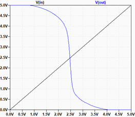
Figure 3: LTSPICE output
Design of the ESD Protection Circuit with chip pads.
|
Figure 4: Nact Pwell Diode
1: (10x80) 2: (68x10) 3: (30x10) |
Figure 5: Pact Nwell Diode
1: (10x80) 2: (68x10) 3: (30x10) |
Figure 6: ESD Pad Circuit (layout) including both diodes.
|
||
|
Figure 4.2: Nact Pwell Diode |
Figure 5.2: Pact Nwell Diode |
Figure 6.2: ESD Pad Circuit (Schematic) |
||


Design of the OPAMP with bias circuit and capacitor
|
Figure 7: Bias Circuit |
Figure 8: Capacitor |
|
Figure 7.2: Bias Circuit |
Figure 8.2: 10pf Capacitor |


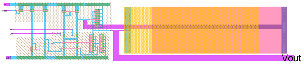
Figure 9: Op Amp
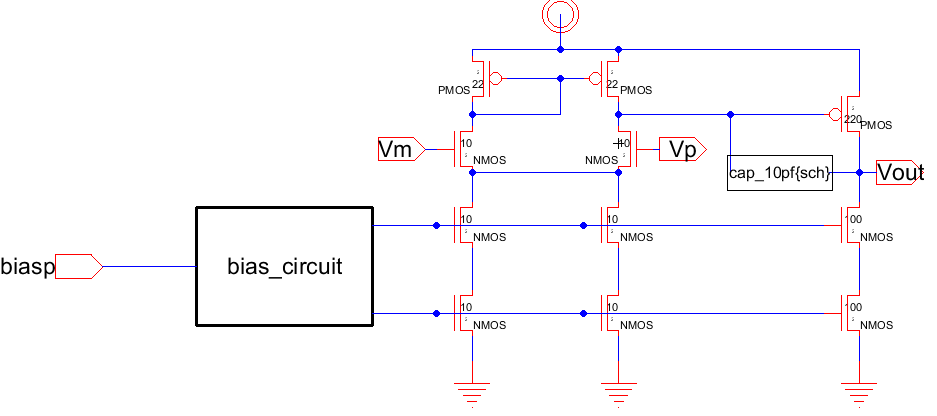
Figure 9.2: Op Amp
All layouts were then imported into the final layout file. Previous iterations of the Pad Frame layout resulted in undetermined DRC errors. Upon redesign of both pad frame and ESD Pad all DRC errors had been resolved.
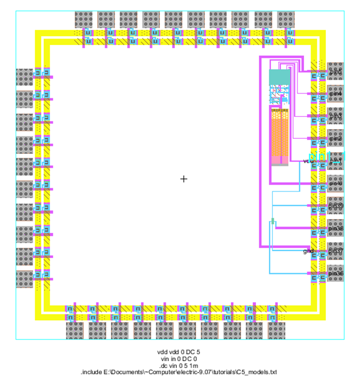
Figure 10: Final integrated circuit layout.
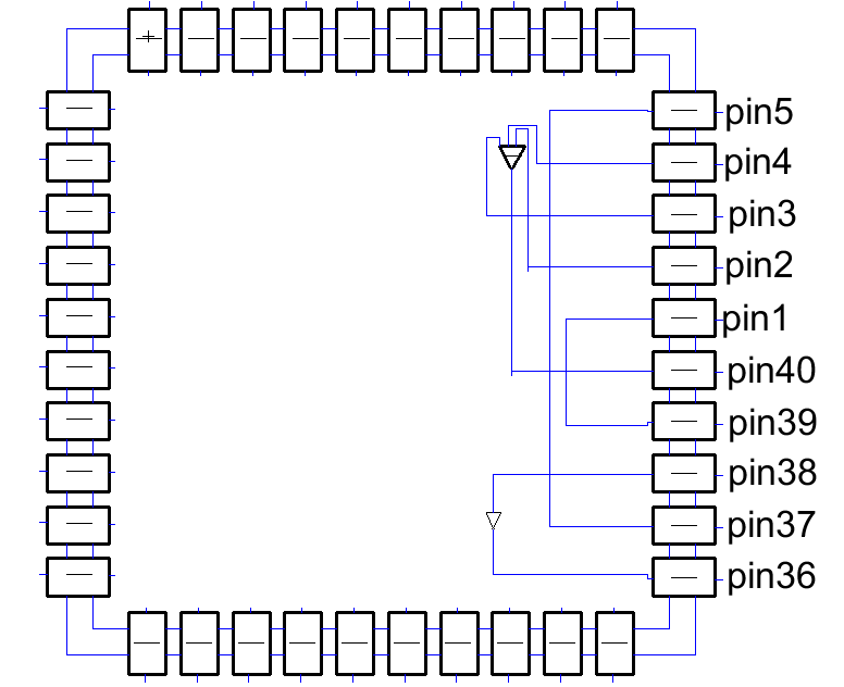
Figure 10.2: Final integrated circuit schematic.
All previous NCC checks ran successfully except for the ESD Pad Circuit (Figure 6), in which Analog_1 failed to match between layout and schematic. This error did not exist before the redesign of the Pad Frame and is expected to have resulted from the attempts to fix the many Pad Frames DRC errors. An attempt was made to redo the entire cell from scratch which fixed all but one missing wire error. The error remained consistent throughout the remainder of the design process. The figure below shows that the error occurred in the OPAMP; but upon further review the error is confirmed to originate from the ESD Pad.


Figure 11: Final DRC and NCC check.
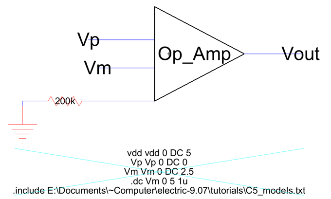
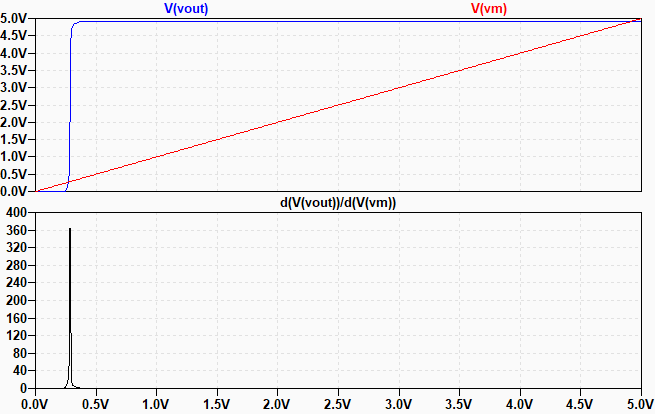
Figure 11: Final simulation of OPAMP
Table 1: Resistor VS Gain
|
Resistor |
Gain |
|
50k |
378 |
|
100k |
380 |
|
200k |
360 |
|
300k |
380 |
Discussion:
Electric VLSI was used to design and simulate an the final OPAMP and all constitutive components. Electric VLSI proved especially useful in its ability to recognize mistakes in the design. Built in error checking tools such as DRC, NCC, and Well Check were used to find mistakes in the schematic and layout. Throughout the lab, many components had to be redesigned in order to resolve errors. All errors were resolved within a reasonable time frame, however the final redesign of the pad frame resulted in an unresolved NCC error. Max OPAMP open loop gain appears to be 380x when using the 200k resistor. It is assumed that full saturation occurs at 100k.