ENGR337 Lab 2020 Spring
Lab 9 Padframe Layout
Name: Kurt Emslie
Email: kdemslie@fortlewis.edu
1. Padframe Layout
2. Introduction
In this lab a padframe was designed and built with electro static discharge protection for the chip.
3. Materials and Methods
Utilizing Electric VLSI a Nact_Pwell diode along with a Pact-Nwell
diode.These diodes were then placed on the a pad and conected
with a metal 3 wire and were placed in a passivation layer. The pad has
six ports that had to be exported. The NCC check ran on each componet
showed that they were clean with out errors. Errors on any of the
componets would not allow proper functioning of the padframe or
subsiquent components. These ports are exprted to the schematic view of
the component. Each component is a layer building on each other until
the padframe was layed out. The pads were made into a 10 segment array
and then that array was copied to make the the subsiquent 3 sides of
the padframe. All of the individual pads in hte arrays had to be
connected to complete teh circuit.The overall size of the pad frame was
1.5mm x 1.5mm. All of the components in this pad frame were DRC and NCC
clean, with no errors.
4. Results
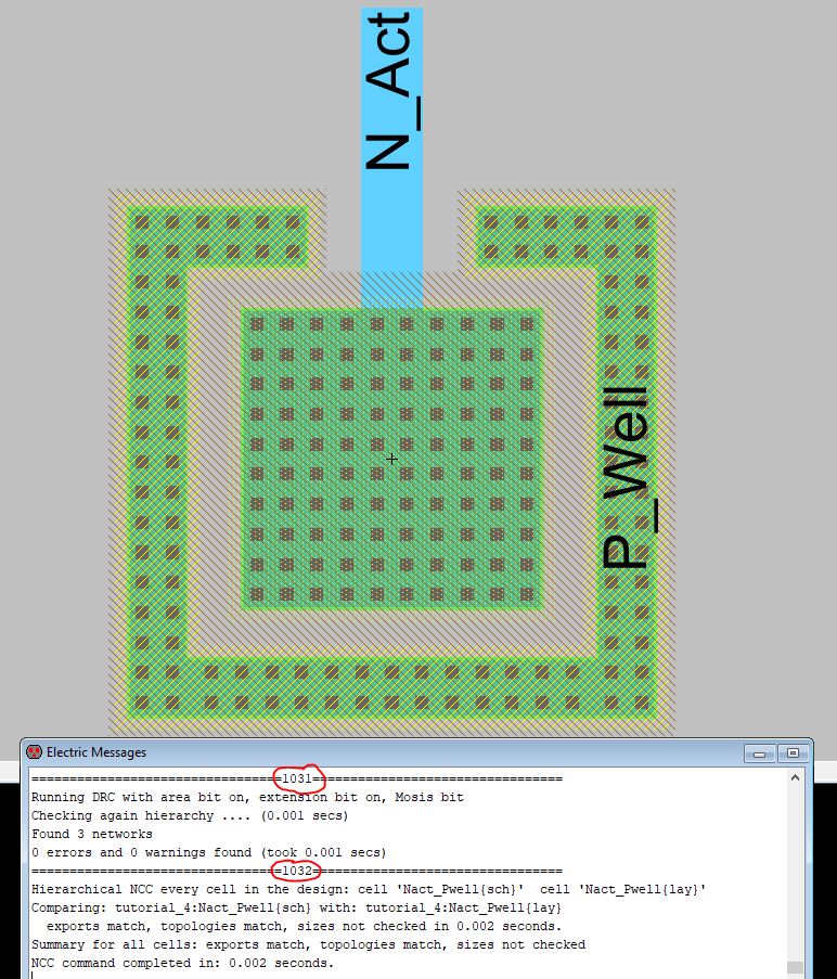
Figure 1: The layout view of the Nact_Pwell and the electric message dialog box showing there were no errors on the component

Figure 2: The schematic view of the Nact_Pwell.
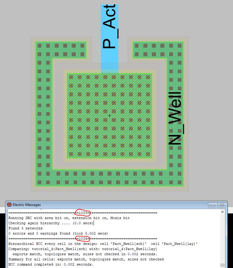
Figure 3: The layout view of the Pact_Nwell and the electric message dialog box showing there were no errors on the component
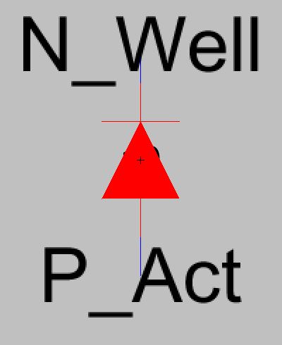
Figure 4: The schematic view of the Pact_Nwell.

Figure 5: The layout view of the pad and the electric message dialog box showing there were no errors on the component

Figure 6: The schematic and icon view of the pad.
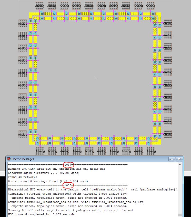
Figure 7: The layout view of the padframe and the electric message dialog box showing there were no errors on the component

Figure 8: The schematic view of the padframe.

Figure 9: The electric message window in Electric VLSI showing there were no errors on any of the components
matching sequentially with the figures above.
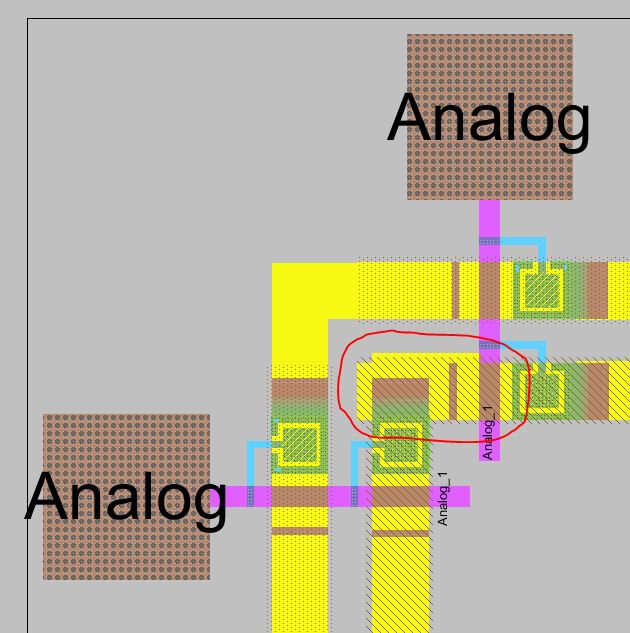
Figure 10: A closer view of the corner conections of the padframe
layout, and the irregularities of the metal 3 after connections were
made.
5. Discussion
This lab was challenging especialy in the
designing of the padframe. Each individual pad that compreised the pad
frame had to be individualy conected to the next in line. When
connecting the inside corners of the metal 3 the size of the metal 3
connectors changed size as shown in figure 10. I was unable to easily
remidy this situation. The padframe was free of RC and NCC errors so
the padframe would effective in its intended purpose. When printing
this chip there would be excess metal 3 printed on the chip. This is
inefficient and would cost extra in the overall production of the chip.
The most important factor in this lab is that the padframe be clean of
all errors, which this design was. The pad frame may not score the
highest points for appearances given the the metal 3 connection son hte
inside corners, but it does recieve full marks for functionality. This
padframe will be implimented in the final design of the chip.