1. Inverter Design
2. Introduction
The purpose of this lab to design and simulate an inverter using PMOS and NMOS transistors.
3. Materials and Methods
The inverter was designed as a schematic and layout in ElectricVSLI, and the simulations of the two configurations were ran using LTSpice. The schematic was designed utilizing NMOS and PMOS transistors, with the drain of the PMOS connected to the source of the NMOS and shorting the gates together. The gates became the input of the inveter in the icon view and the conection between the source and drain of the transistors became the output of the inverter in the icon view.
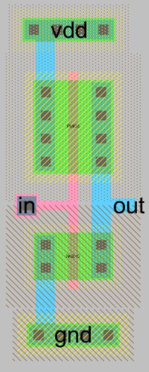
The layout of the invertor was designed with the PMOS and NMOS transistors along with two Pact's and Nact's serving as pins for the source and drains of the transistors. Pwells and Nwells were also added to the complete the circit. Simulation of the schematic and the layout versions of the inverter were ran using LTSpice.
4. Results

Figure 1: The schematic of the inverter.
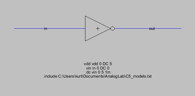
Figure 2: The icon of the inverter containing the schematic of the inverter.

Figure 3: The results of running the simulation of the inverter schematic in