ENGR337 Lab 2020 Spring
Lab 5
Name: Kurt Emslie
Email: kdemslie@fortortlewis.edu
1. Rectifiers, DC Regulators, and Voltage Doubling Circuits.
2. Introduction
Thge purpose of this lab was to design an build rectifiers, DC
regulators and a DC power supply on a bread borad and using simulation
software, LT Spice. This lab will provide a us with an opportunity to
better understand the behavior of these circuits as well as understand
how intoducing diodes into circuits effects the behavior of the circuit
and the resulting outputs.
3. Materials and Methods
The first circuit built, simulated, and tested in this lab was a half
wave rectifying circuit. The circuit was comprised of a 1k resistor, a
1N 5767 diode, and was simulated with a 10V vpp sine wave in put at a
frequency of 1 kHz.
The second circuit built, simulated and tested was a DC regulating
circuit. It was comprised of a 1N 5767 diode, a 33 uF capacitor and a
1k resistor in parallel and was driven by a 8V vpp sine wave at a
frequency of 1 kHz.
The third circuit was comprised of a 1k resister, aforward bias and
reverse bias diodes in parallel and was driven by a 10V vpp sine wave
with a frequency of 1 kHz. This circuit was a combination of two half
wave recitifiers.
The fourth ciruit built was comprised of two 1N 3733 zener diodes, one
forward and one reverse biased, in series with 1k resistor, driven by a
40 V vpp sine wave at a frequency of 1 kHz. This configuration of the
circuit would clamp of restict the voltage in the circuit.
The fifth and final circuit built, simulated and tested in this lab was
a voltage boubling circuit. This circuit was comprised of two 1 uF
capacitors, and two 1N 5767 diodes driven by a 10 V vpp sine wave at a
frequency of 100 Hz.
4. Results
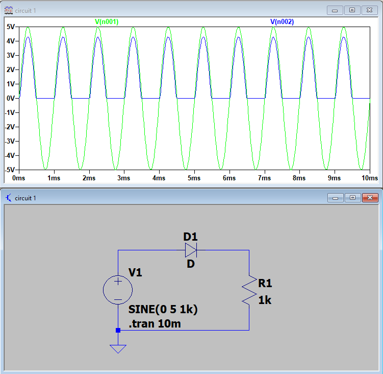
Figure 1. The LTSpice simulation of the half wave rectifier.
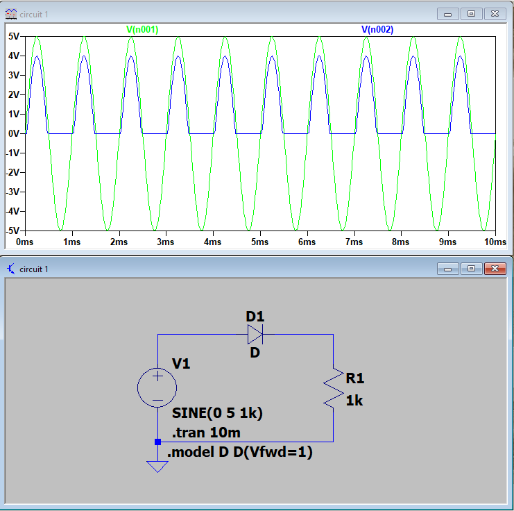
Figure 2. The LTSpice simulation of the half wave rectifier with a bulit in voltage of 1 Volt.
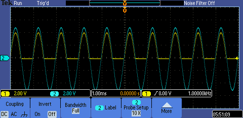
Figure 3. Testing the half wave rectifier circuit built on the breadboard with the oscilloscope.

Figure 4. LT Spice simulation of the DC converter circuit.
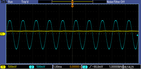
Figure 5. Testing the DC converter circuit built on the breadboard with the oscilloscope.
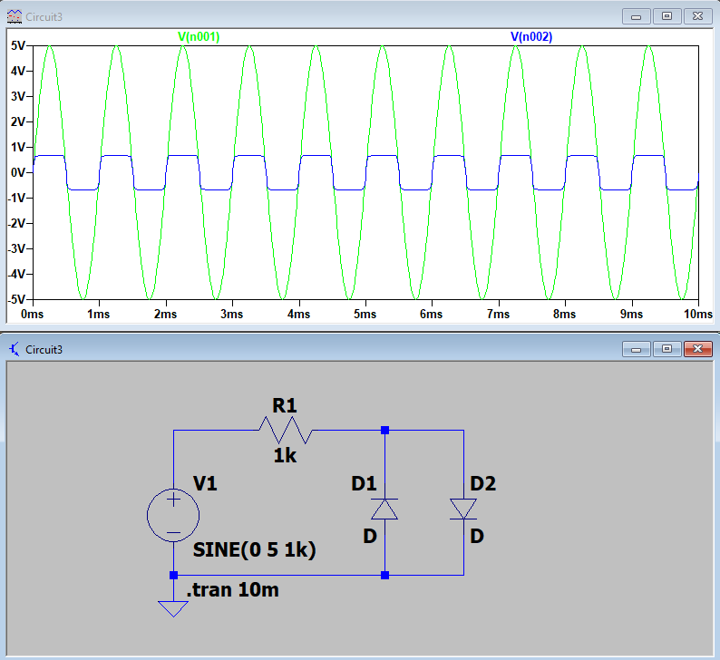
Figure 6. The LT Spice simulation of the circuit with two half wave rectifiers.
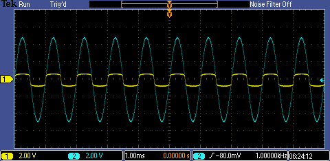
Figure 7. Testing the circuit with two half wave rectifiers that was built on the breadboard with the oscilloscope.

Figure 8. The LT Spice simulation of the circuit with two diodes clamping the voltage.

Figure 9. Testing circuit clamping the voltage that was built on the breadboard with the oscilloscope.

Figure 10. LT Spice simulation of the voltage doubling circuit.
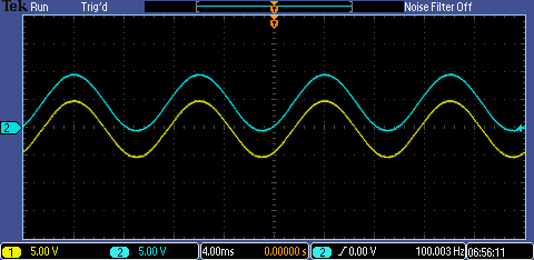
Figure 11. Testing the initial output voltage of the doubling circuit that was built on the breadboard with the oscilloscope.
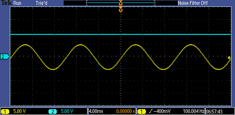
Figure 12. Testing the
final doubled output voltage gernerated by the doubling circuit that
was built on the breadboard with the oscilloscope.
5. Discussion
Testing
and simulation of the half wave rectifying circuit showed that
when input voltage to the circuit dropps below 0V the current through
the diode is stopped. When the input voltage to the circuit is above 0V
current is alllowed to flow through the diode, but does not reach the
full value of the input signal. This delta in the voltage is due to the
built in voltage the diode has.
Testing on the DC converting circuit resulted in differences between
the LT SPice simulation of the circuit and testing the circuit bulit on
the bread board. This is potentialy due to the power supply or the
frequency of the input signal, not being adequate to fully charge and discharge the capacitor.
Testing of the doubled half wave circuit indicated the effects of
forward and reverse bias on diodes and how they limit the voltage with
in the circuit.
Testing of the fourth circuit showed how the combination of the two
zener diodes limited the voltage in the circuit above and below the
break down voltage values of the diodes. Testing showed the break down
voltage to be approximately 5V.
The last circuit tested was the voltage doubling circuit. The
configuration of this circuit allowed the singnal to go through a
forward biased diode and a capacitor to raise the voltage. Then the
signal went through an other forward biased diode and capacitor, that
doubled the original signal value. Figure 10 shows how the original
signal of 5V vpp was altered, esentialy cutting off the bottom of the
signal around 0V and then using that bottom half of the signal to
amplify the ending value of the signal to 10V.