ENGR337 Lab 2018 Spring
Lab 2 ENGR 337 Analog Electronics
Name: Kurt Emslie
Email: kdemslie@fortlewis.edu
1. LTSpice and the Compensated probe.
2. Introduction
This lab gave us more experience running simulation on circuits in LTSpice. It also introduced us to
the oscilloscope as another tool to analyze circuits with. We also
investigated what comprised the compensated probe on the oscilloscope
to better understand its ability to filter out certain frequencies.
3. Materials and Methods
For this lab LTSpice was used to to simulate the response of the first
five circuits. The attributes of the input signal were changed in each
subsequent circuit until the capacitor was able to reach the voltage
supplied by the input signal. The size of the resistor and capacitor
were also changed to allow the capacitor to fully charge. The next
circuit tested was built on a bread board using a 1k resistor and a
100pF capacitor. A signal generator provided a 5V input square wave to
the circuit. An oscilloscope was used to read the Vin and Vout signals
on the circuit to determine the time delay of the between the signals.
Another circuit was built on the bread board with a 100k resistor and a
680pF capacitor. This circuit was given a sine wave input signal with
amplitude of 5V. The time delay and attenuation of the circuit were
found with the oscilloscope as well as through simulation of the
circuit in LTSpice, and by calculating them by hand. The final circuit
tested replicated a compensated probe, where the value of the resistor
in the DC component had to be calculated, then the circuit was tested
with the resistor. Then the capacitor in the AC component of the
circuit had to be calculated and simulation ran on the circuit. These
tests were to demonstrate the how the internal resistance and parasitic
capacitance of the circuit magnify the attenuation of the signal in the
probe.
4. Results

F1: LTSpice simulation of the first circuit.

F2: LTSpice simulation of the second circuit.

F3: LTSpice simulation of the third circuit.
F4: LTSpice simulation of the fourth circuit.

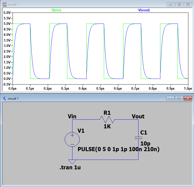
F5: LTSpice simulation of the fifth circuit.
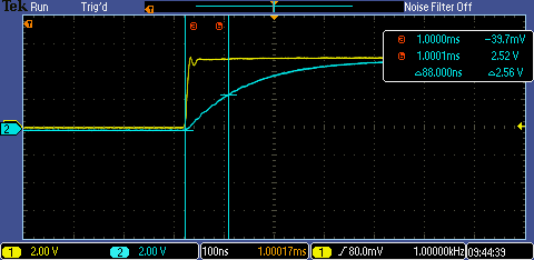
F6:The time delay measure by the oscilloscope on the sixth circuit built on the bread board with a square wave input.
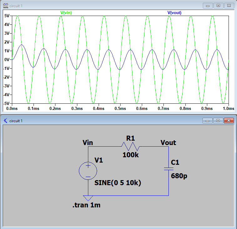
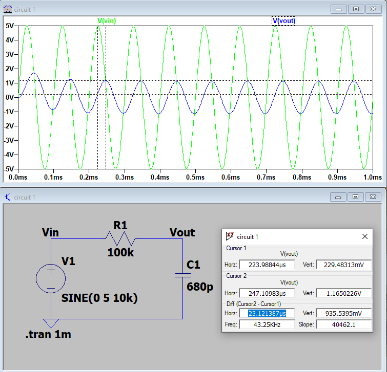
F7: LTSpice simulation of the sixth circuit.
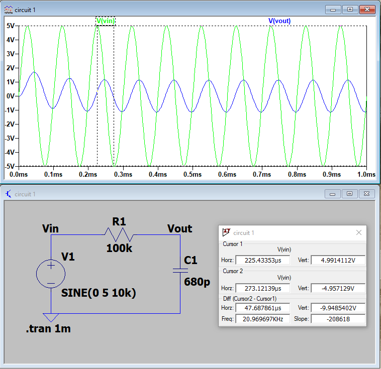
F8: The time delay of the sixth circuit.
F9: The Vi signal of the sixth circuit.

F10: The Vo signal of the sixth circuit.

F11: The hand calculation of the time delay and attenuation of the sixth circuit.

F12: The time delay of the sixth circuit as measure by the oscilloscope.
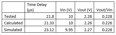
T1: The results of the tested, calculated and simulated time delay and attenuation of the signal in the circuit.

F13: Hand Calculations for the resistor and capacitor values for the 10x compensated probe.
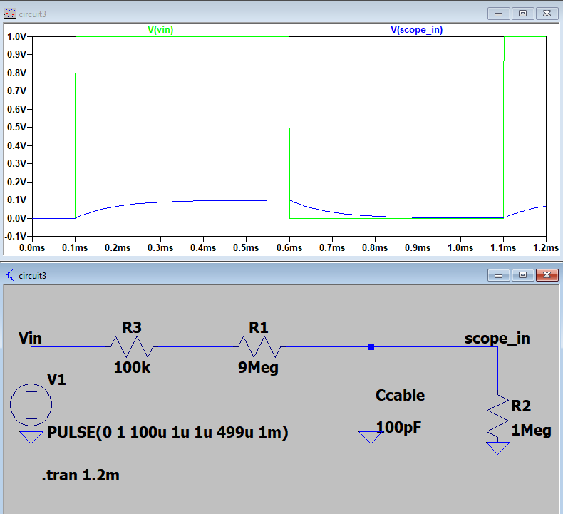
F14: The LTSpice simulation of the compensated probe circuit with 10x DC attenuation.

F15: The LTSpice simulation of the compensated probe circuit with 10x AC and DC attenuation.
5. Discussion
The scope of the first five circuits tested was to demonstrate how the
set points of the input signal and the size of the components can
effect a capacitors ability to charge and discharge. In Figure 1 the
time delay is so large that it does not allow the capacitor to reach
the full amplitude of the input signal. Figure 2 demonstrates how
increasing the amplitude of the voltage seen by the capacitor does
nothing to increase the amount of voltage absorbed by the capacitor. In
Figure 3, a increase in the frequency of the signal does allow the
capacitor to see the full amplitude of the input signal. It is also
demonstrated iF8: The results of the tested, calculated and simulated time delay and attenuation of the signal in the circuit.n
Figures 4 & 5 that reducing the size of the capacitor and resistor
and also enable the capacitor to see the full amplitude of the input
signal.
The sixth circuit was given a square wave input and when tested with
the oscilloscope, the time delay was measure to be 88ns. The circuit
was then given a sine wave with a frequency of 10kHz. The time delay of
the signals and the attenuation were then simulated in LTSpice as shown
in Figures 8 - 10. The time delay and attenuation were calculated by
hand, show in Figure 11. Then there were recorded from the oscilloscope
when testing the circuit, shown in Figure 12. The results shown in T1,
show that the 3 different methods were able to come to extremely close
values. This validates the time delay and attenuation of the signal as
to being good values.
The last circuit tested was the representation of the compensated probe
of the oscilloscope. This test was to learn how the internal resistance
and parasitic capacitance of the circuit effect the attenuation of the
signal. In Figure 13 the values for the resistor and capacitor were
calculate by hand for the circuits. The results of the simulation of
the DC component of the circuit is show in Figure 14. The results of
the simulation of the AC and DC component of the circuit are shown in
Figure 15.