ENGR337 Lab 2018 Spring
Lab 1 LTSpice Circuit Analysis
Name: Kurt Emslie
Email: kdemslie@fortlewis.edu
1. LTSpice and Lab Report Preparation
2. Introduction
In this lab we analyzed 5 different circuits and recorded the
results. On circuit 1 we calculated the voltage and current
across the circuit by hand with mesh analysis. We compared that with
what we tested the voltage and current on the circuit with a multi
meter. We also entered the parameters of the circuit into LTSpice and
recorded those values and compared all three values.
The second circuit was analyzed the circuit in LTSpice comparing the
time-delay and amplitude attenuation of the output signal to the input
signal.
In the third circuit we preformed a transient analysis of the of the
circuit using the DC sweep function in LTSpice. The voltage was varied
from -2V - 5V, and the input and output signal were compared.
The fourth circuit was analyzed with the AC sweep function in LTSpice.
This analysis would look at the frequency of the input and out put
signals within the circuit and allow the bandwidth of these signal to
be compared.
The fifth circuit was analyzed with the DC pulse function in
LTSpice to simulate driving a capacitor. The time delay between
the input and output signals were compared in this experiment.
3. Materials and Methods (Do not simply list everything there, put them in a table if needed).
The materials used in this lab were a bread board, 3K and 2K resistors,
multimeter, LTSpice, Excel and a calculator for the calculations done
by hand.
4. Results (Your data/figure should have a caption. Figures should be labeled/numbered.)

F1. The circuit that was built and the voltage a current was calculated, tested and simulated across the circuit

F2. The nodes where the voltage was tested, calculated, and simulated on the circuit and the circuit.

F3. The hand calculations of the mesh voltage method to calculate the voltage in the circuit.

F4. The results of testing, measuring and simulating the voltage and current across the circuit.

F5. The results of comparing the time-delay and amplitude attenuation of the output signal to the input signal on circuit 2.

F6. The voltage of the input signal on the second circuit.
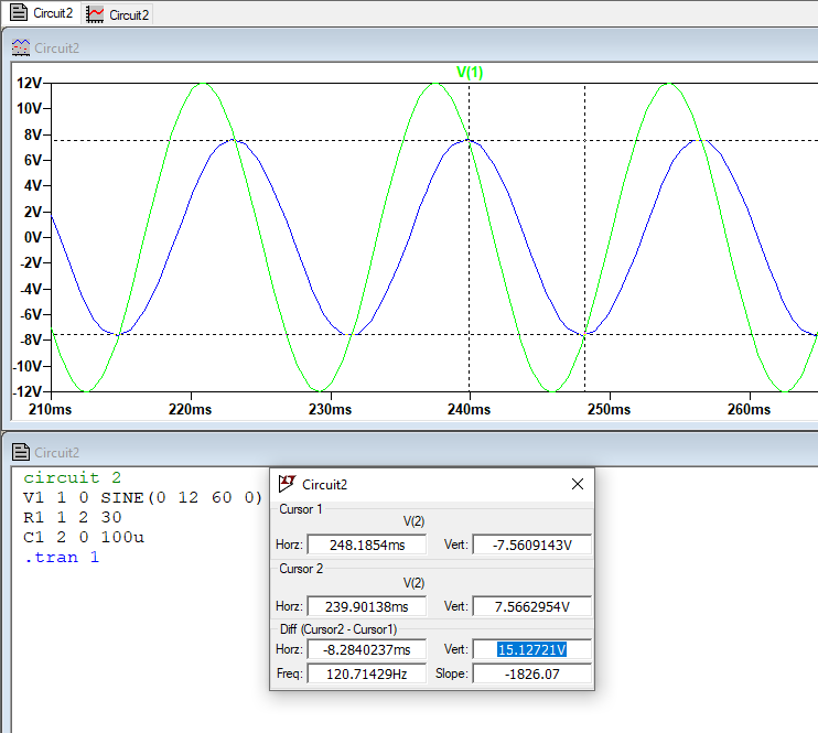
F7. The voltage of the output signal on the second circuit.

F8. The
results of the transient analysis of the circuit with the DC
Sweep function and the comparison of the input and output signals on
circuit 3.
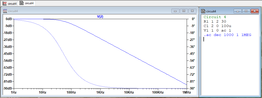
F9. The results of the analysis of the circuit with the AC sweep
function, and the resulting band width of the input and output signals
on circuit 4.

F10. The results of the DC pulse function on circuit 5 and the measured time delay between the input and output functions.
5. Discussion
The results of the analyzing circuit 1 shown
in F3, indicate that all three methods were very
close to each other. This verifies that all thee methods were a viable
means of analyzing the circuit, and that the calculations were verified
to be accurate. Using a sine wave as the input signal in circuit 2
shows F4, F5, F6 show the time delay and voltage difference between the
input and output signals of the circuit. Circuit 3 was analyzed
using the DC sweep function with the input voltage varying fro -2V -
5V. F7 shows the linear results of the function and the voltage was
increased in the circuit. There were no components in the circuit to
cause a time delay between the input and out Using the AC sweep
function circuit 4 was analyzed. F8 shows the band width of the input
and output signals of the circuit. Circuit 5 was analyzed with a DC
pulse function representing the loading of a capacitor, the time delay
between the input and output signals are shown in F9. The time delay
was also calculated by hand with the formula, td = 0.07*RC. It was
calculated to be 19ns, and on the simulation it was shown to be 21ns.