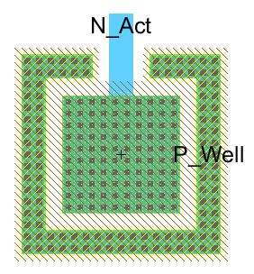
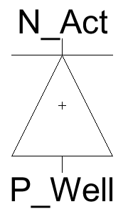
ENGR337 Lab 2020 Spring
Lab 9 Complete Tutorial 4
James Ferguson
jwferguson@fortlewis.edu

Lab 9 Complete Tutorial 4

Objective:
The goal of this lab is to design a pad frame with electro static dischardge (ESD) protection for production of an integrated circut chip with an inverter inside as well as gain experiance with the software ElectricVLSI.

Methods:
ElectricVLSI was setup prior to starting followintg the same procedure as in Lab 6. This report follows instructions found in Tutorial 4:  Layout the padframe on Dr. Li's website.

Nact_PWell_diode
:
Layout and Schematic of a P-well based diode.
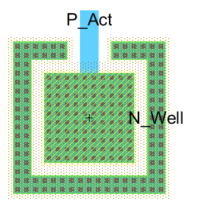
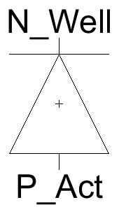

Pact_NWell_diode:
Layout and Schematic of a N-well based diode.
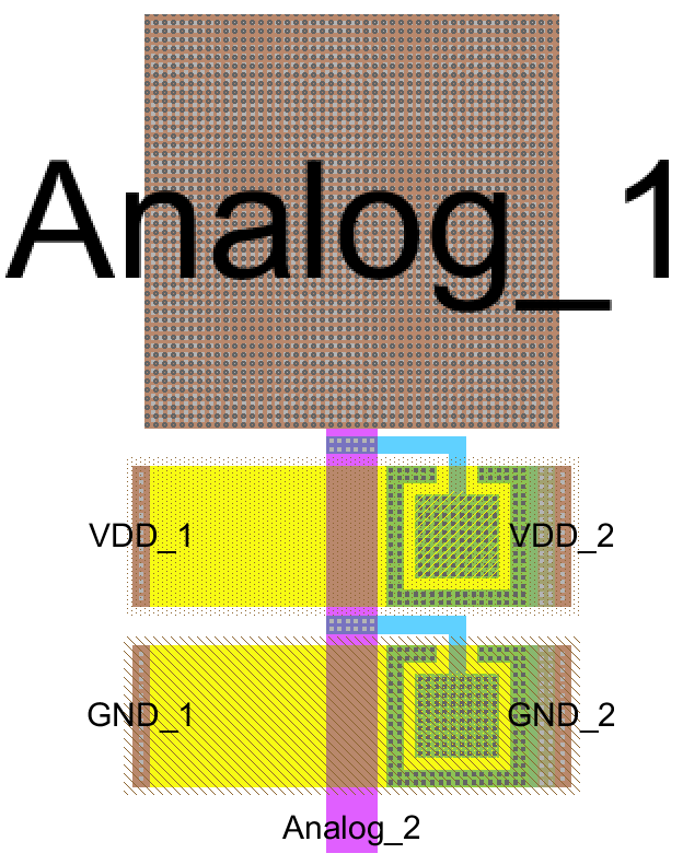
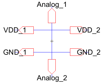
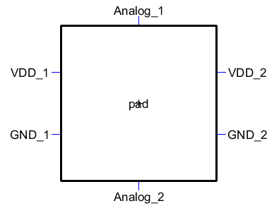

pad:
Layout and Schematic for a pad with ESD protection.
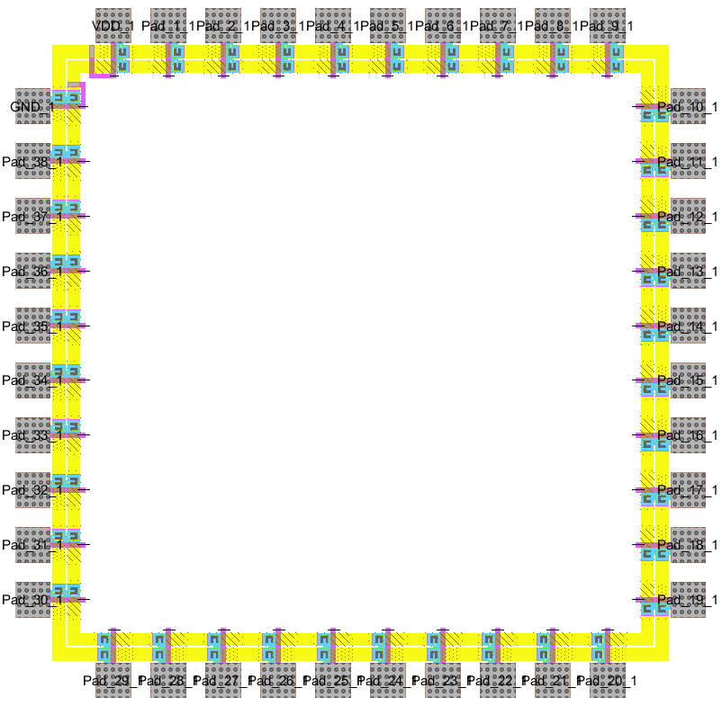

pad_frame:
Layout and Schematic for a pad fram ESD protection with pads for VDD, GND, and 38 generic pads.


inverter_20_10_pad:
The inverter designed in Lab 8 placed inside a pad frame with ESD protection.


Discusion:
All layout and schematics passed  DRC, ERC, and NCC tests without any errors and apper to be usable. Having a pad frame layed out will be usefull for reuse in the future when designing integrated circuts.