ENGR337 Lab 2020 Spring
Lab 8 Complete Tutorial 3
James Ferguson
jwferguson@fortlewis.edu

Lab 8 Complete Tutorial 3

Objective:
The Goal of this lab is to design a MOSFET based inverter in ElectricVLSI as well as gain experiance with said software.

Methods:
ElectricVLSI was setup prior to starting followintg the same procedure as in Lab 6. This report follows instructions found in Tutorial 3: Layout an Inverter on Dr. Li's webcite. The following shows the scematic, layout and LTspice simulation designed of the designed inverter. A inverter works by combining a NMOS MOSFET and PMOS MOSFET such that the input is connected both gates. When the input is pulled high the NMOS pulls the output low, when the input is pulled low, the PMOS pulls the output high.

Inverter Schematic:
The inverter designed has a PMOS with a width of 20 and a NMOS with a width of 10.


Inverter Schematic Simulation:


The circut  performed as expected.

Inverter Layout:
The inverter layout constists of a PMOS MOSFET and NMOS MOSFET.

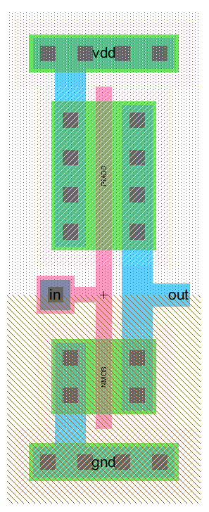
The designed layout passed DRC, ERC and, NCC with no errors.

Inverter Layout Simulation:


The circut  performed as expected.


Discusion:
The inverter performed as expected in both the schematic and layout simulations with vout being high given a low vin and vice verca.