ENGR337 Lab 2020 Spring
Lab 7 Layout an NMOS and PMOS
in ElectricVLSI
James Ferguson
jwferguson@fortlewis.edu
Lab 7 Layout an NMOS and PMOS in ElectricVLSI
Objective:
The Goal of this lab is to design a NMOS and PMOS MOSFETs in ElectricVLSI as well as gain experiance with said software.
Methods:
ElectricVLSI was setup prior to starting followintg the same procedure as in Lab 6. This report follows instructions found in Tutorial 2: MOSFETs and IV Curves on Dr. Li's webcite. The following shows the scematic, layouts and LTspice simulations designed of NMOS and PMOS MOSFETs.
NMOS:
NMOS Schematic:
g is the MOSFET gate, d is the MOSFET drain and s is the MOSFET source.

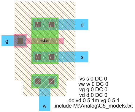
NMOS Layout:
The NMOS layout consists of an 'nMos', 2 'nAct's, a 'pWell', and a mettal node.
g is the MOSFET gate, d is the MOSFET drain, w is the MOSFET ground and s is the MOSFET source.
NMOS Results:
The
following shows the simulated curent flowing from the source to drain
current of the designed NMOS as a function of gate voltage.
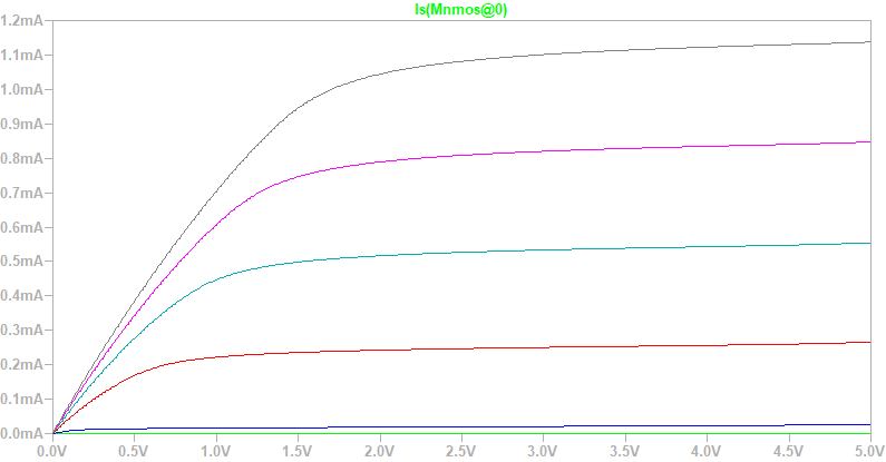 The circut performed as expected.
PMOS:
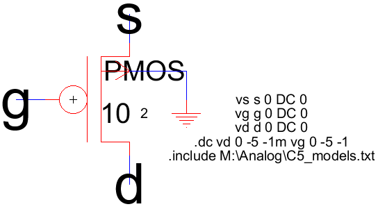
PMOS Schematic:
g is the MOSFET gate, d is the MOSFET drain and s is the MOSFET source.
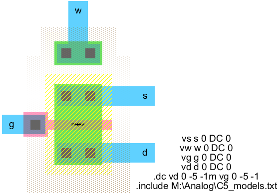
PMOS Layout:
The
PMOS layout consists of an 'pMos', 2 'pAct's, a 'nWell', and a mettal node.
g is the MOSFET gate, d is the MOSFET drain, w is the MOSFET ground and s is the MOSFET source.
PMOS Results:
The following shows the simulated
curent flowing from the source to drain current of the designed PMOS as
a function of gate voltage.
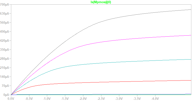 The circut performed as expected.
Discusion:
The MOSFETs designed in this lab performed as expected with currents leveling out in the saturation region and experiance with ElectricVLSI was gained.