ENGR337 Lab 2020 Spring
Lab 9 Padframe Layout
Name: Jessica Shinkle
Email: jlshinkle@fortlewis.edu
1. Title: Padframe Layout
2. Introduction
In this lab a padframe was designed and built in the Electric program.
3. Materials and Methods
Electric
VLSI software was used to build the padframe of a chip. First a Nact_Pwell
diode and a Pact_Nwell diode were created using the layout and schematic view
in the software. To prevent a burnout due to ESD on the chip these diodes were
combined. They were wired up to a pad. The ESD pad has six inputs / outputs.
They are the VDD input and output, the GND input and output, and the analog
connections. Once all of the inputs and outputs were exported they were then
made in a schematic view.
The
pads are then brought into a layout view and made into a 10 segment array. To
make the subsequent 3 sides of the padframe the 10 segment array was copied and
utilized. To make sure the components were running properly a DRC and NCC
check.
4. Results
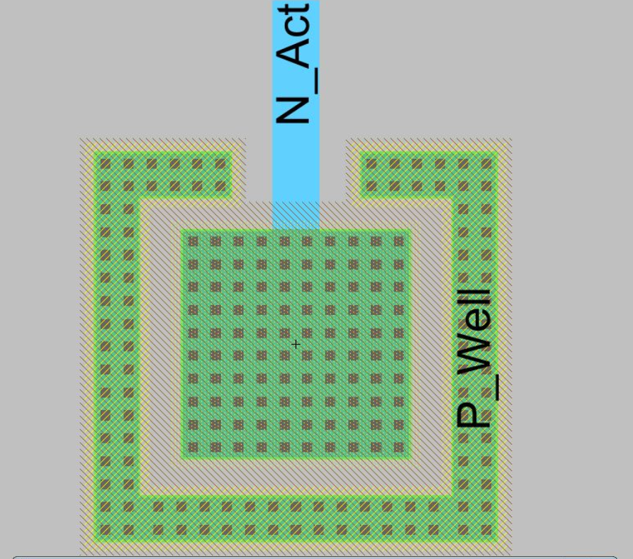
Figure 1: Nact_Pwell in the layout view
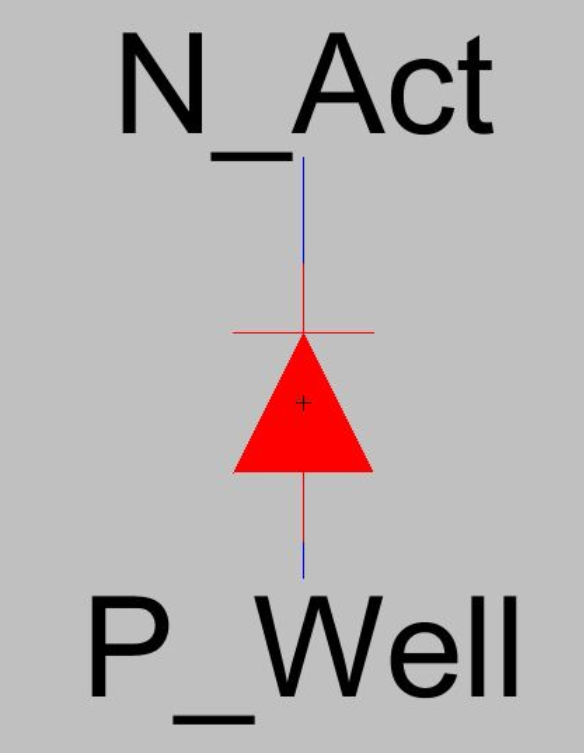
Figure 2: Nact_Pwell in the schematic view
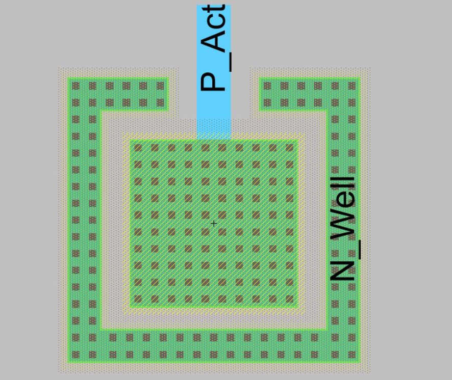
Figure 3: Pact_Nwell in the layout view
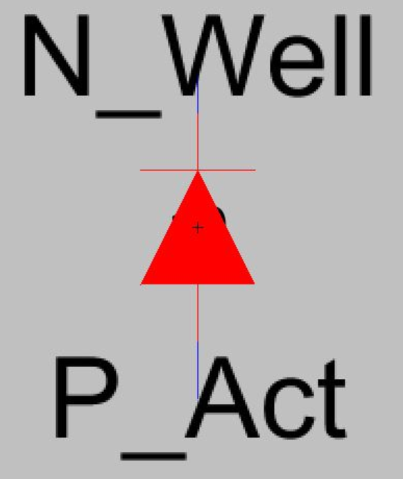
Figure 4: Pact_Nwell in the schematic view
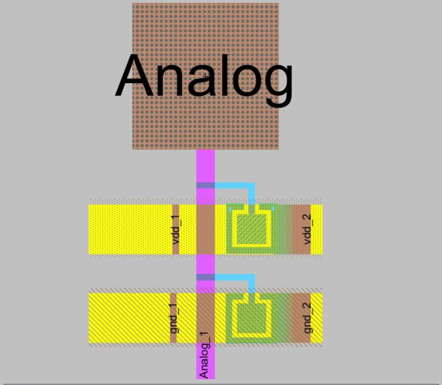
Figure 5: Pad in the layout view
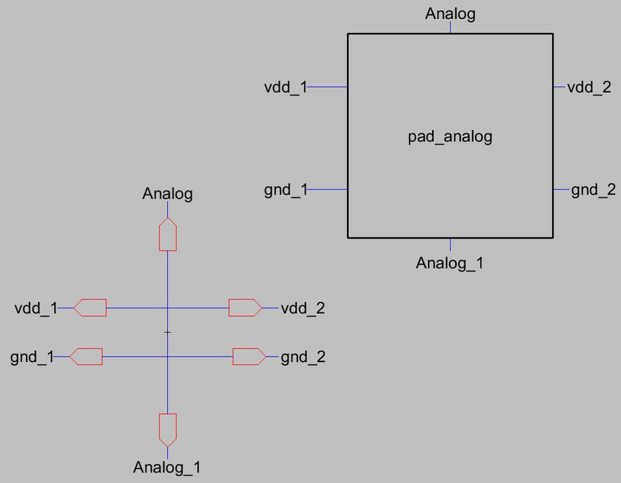
Figure 6: Pad in the schematic and icon view
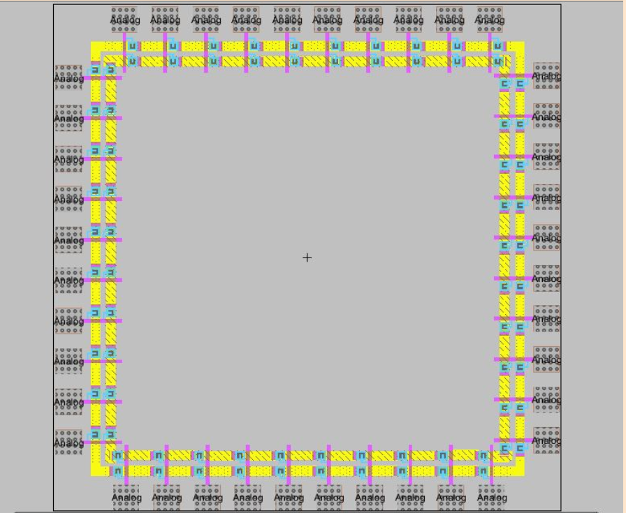
Figure 7: Padframe in the layout view
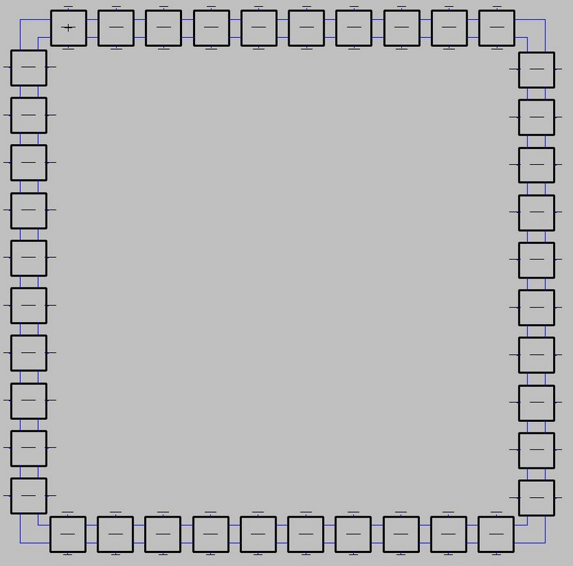
Figure 8: Padframe in the schematic view
5. Discussion
This lab was succeful in making the padframe
for the chip. This padframe has an extra feature that protects the chip
from extra voltages. This will be super benificial when this chip is
used in real applications. It was definityley really difficult in the
desinging of the padframe.