1. Lab 8: Layout an Inverter
2. Introduction
The goal for this lab was to use Electric VLSI to layou an inverter using PMOS and NMOS transistors.
3. Materials and Methods
To start tutorial_2 was copied and renamed tutorial_3. This was to copy the nMos node instead of starting from scratch. Next a new cell was created and named inv_20_10. The nMos node that was coppied was pasted into this cell and changed to a transistor. This was repeated for the pMos node in the cell PMOS_IV. The width of the pMos was also changed to 20. On the PMOS cell a power and gnd symbol were added and connected accordingly. Two off grid nodes were connected into the system and exported as input and output nodes.
Next an icon view was created for this schematic. This icon view was changed so that it looked like an inverter. Once the icon view was created the operations of this inverter was simulated. A schematic called inverter_sim was created and the icon was placed into this schematic. To simulate the inverter LTSpice code was added and run through that program.
The layout view of the inverter was created next meaning there are three view in the inv_20_10. Within this view one nWll node and pWell node were placed in it. Two pAct nodes and nAct nodes, and a pMos and nMos nodes were also placed within this view. The width of the PMOS was set to 20 and the width of the NMOS was set to 10. The x-size of both pAct Nodes were set to 20 and both nAct Nodes were set to 10. Everything was formated and connected accordingly before a poly1 to metal1 contact and meatal1 Pin were placed within the view. Again these were connected and formated accordingly into the view. Before simulating the layout vdd, in, and out nodes were exported into the view in the correct places. The inverter_sim cell was created with a layout view and the inv_20_10{lay} was dragged into the drawing area. Arcs were added into the view and named/exported accordingly. Once LTSpice code was added the view was simulated within the program.
4. Results
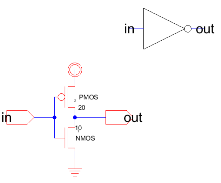
Figure 1: Schematic view within the inv_20_10 cell
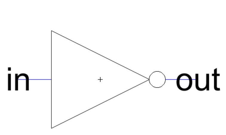
Figure 2: Icon view within the inv_20_10
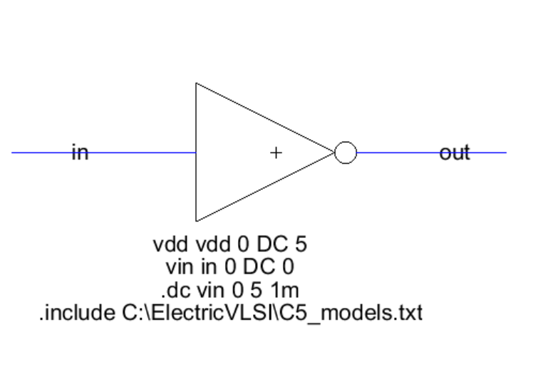
Figure 3: Icon view within the inverter_sim_ic view
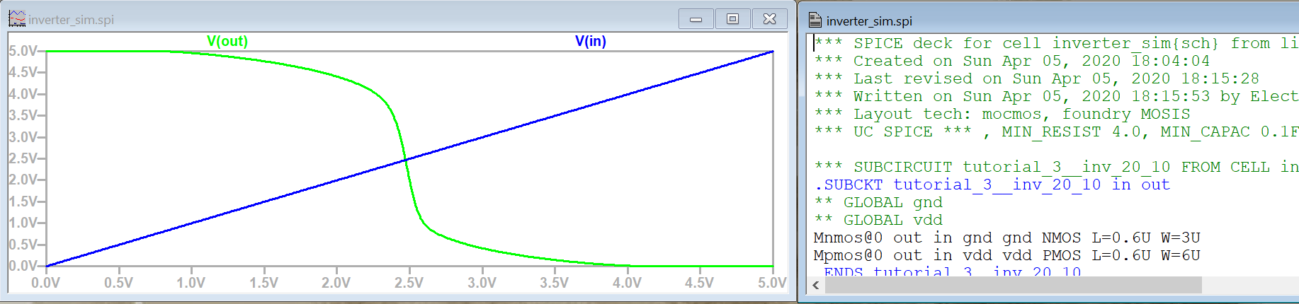
Figure 4: LTSpice simulation for the inverter_sim_ic view
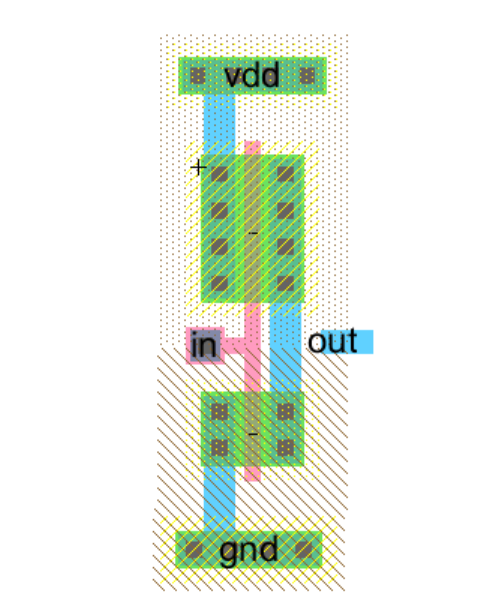
Figure 5: Layout view for the inv_20_10 cell
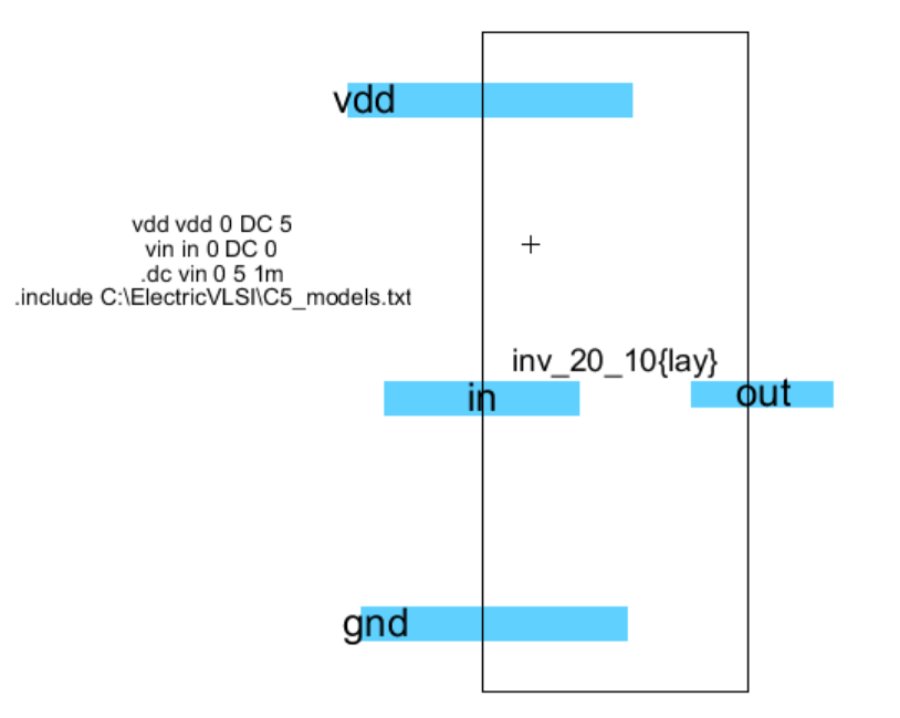
Figure 6: Layout view within the inverter_sim cell
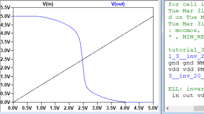
Figure 7: LTSpice simulation for the inverter_sim_lay view
5. Discussion
The inverter was successfully created using both the schematic and layout views within the program. This lab used a lot of tools that were taught in the previous labs and some new tools aswell. The exporting tool was a new and useful method used in this lab. Overall this was a great lab and very insightful.