This lab was the first titorial to help us figure out how to do the layout of an N-Well resistor and voltage divider in Electric VLSI.
3. Materials and Methods
To do this lab, Java and Electric VLSI were downloaded. Once they were downloaded the intruction within the titorial were followed to fix all the setting with in the programs. After all the settings were fixed and the file was saved to the c drive an n-well resistor and voltage divider was created in the progam. The directions of how to do so were given by the intructor. In Electric VLSI we learned how to use some of the tools in the schematic view and the layout view. The voltage divider was made in the schematic view and the n-well resistor was made in the layout view. Once these were made, graphs of the input and output voltage of both were run in LTSpice.
4. Results
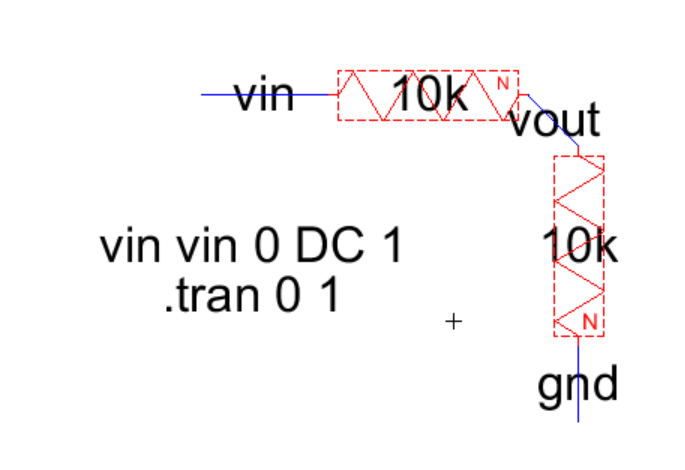
Figure 1: The view of the voltage divider in the schematic view
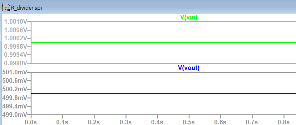
Figure 2: The input and output voltage of the voltage divider in LTSpice
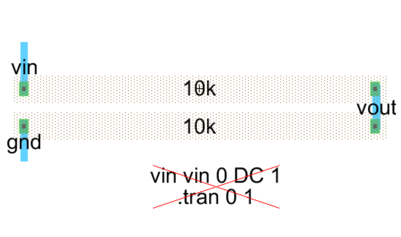
Figure 3: The n-well resistor in the layout view
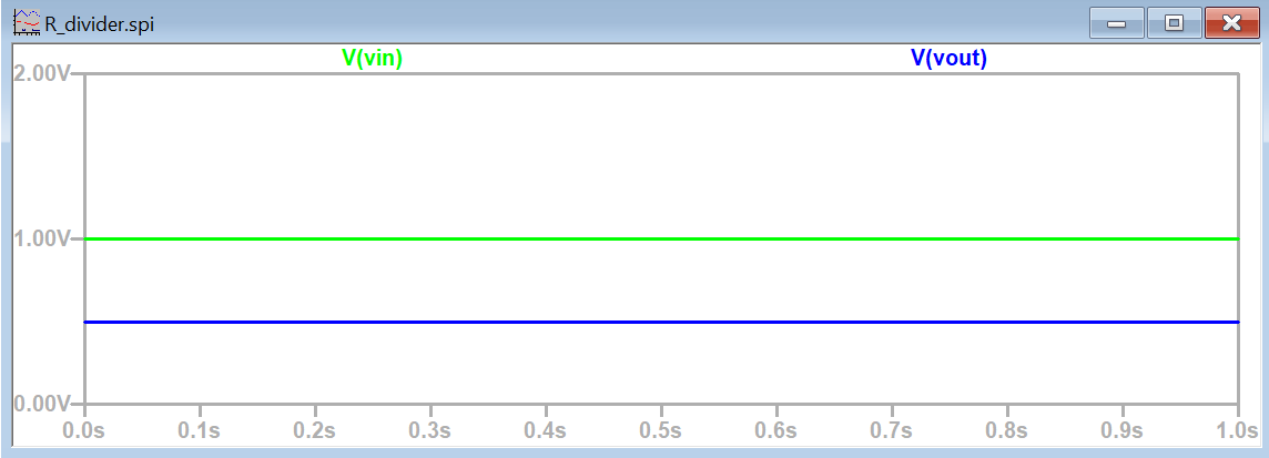
Figure 4: The input and output voltage of the n-well resistor
5. Discussion
This lab was very helpful in teaching me how to navigate through the new program. The titorial showed us how to use the layout and schematic layout integraded into the program. It was also really cool how we could incorperate LTSpice into the new progam as a graphing tool. An important lesson that was learned is to check for errors frequently while making the circuit. This way we can catch a mistake early and fix it as necessary.