ENGR337 Lab 2020 Spring
Project
Name: Jessica Shinkle
Email: jlshinkle@fortlewis.edu
1. Title - Project
2. Introduction
This Project used the accumulated knowledge from
both class and labs to produce a functioning inverting Op-Amp. Using
LTSpice as the chip design software the final result needed to be both
DRC and NCC clean to ensure that the chip layout was functioning design.
3. Materials and Methods
Using Electric program a bias was design to be later used in the inverting
op-amp. Therefore the N-wells and P-wells where placed far enough
apart to encompass the width of the capacitor later in the project.
With the bias designed it an op-amp was made and the bias was overlad
on both the schematic and layout. With the op-amp finalized a capacitor
and resistor were place into the circuit to make it an inverting
amplifier. The inverting amplifier was checked for any NCC and DRC
error, if clean the inverting amplifier was placed into the chip
schematic finalizing the project.
4. Results
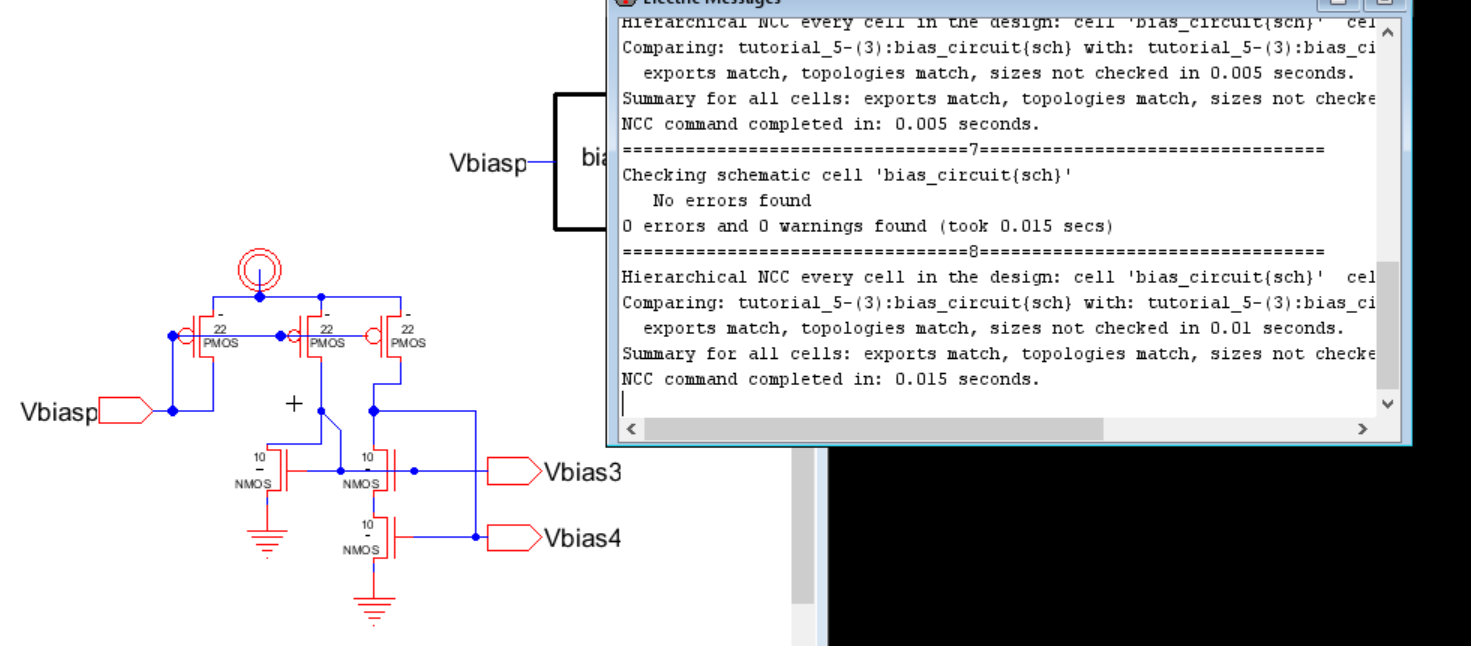
Figure 1: The bias within the circuit in the schematic view
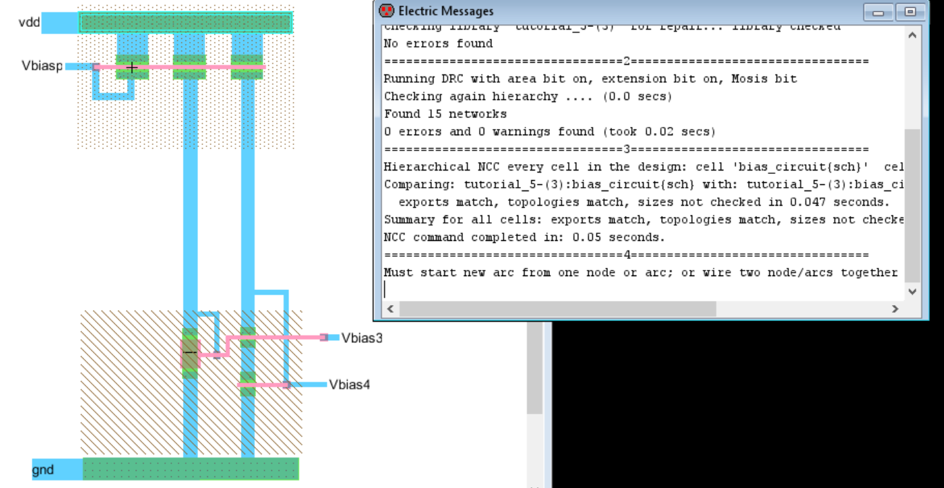
Figure 2: The bias within the circuit in the layout view

Figure 3: The capacitor in the schematic view

Figure 4: The capacitor in the layout view
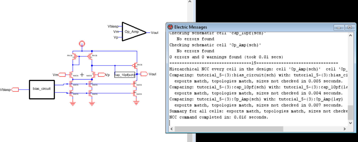
Figure 5: The Op-amp in the schematic view
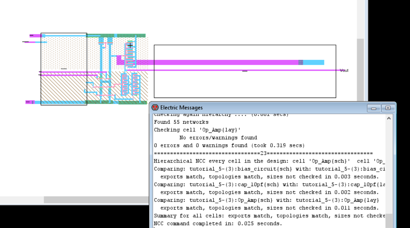
Figure 6: The Op-amp in the layout view
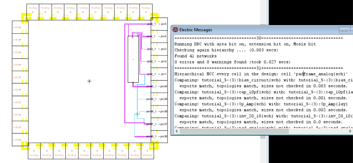
Figure 7: The padframe in the layout view
5. Discussion
This project was definitly time consuming
but super informing. Dobbs and I had some troubles with the NRC check
in the very end but reached out for help. Overall this lab was a
success and everything worked properly in the end as seen in the
figures.