ENGR337 Lab 2020 Spring
Lab 5
Name: Jessica Shinkle
Email: jlshinkle@fortlewis.edu
1. Lab 5: Rectifiers and DC Regulators
2. Introduction
This lab should help familiarize our selves with the Rectifiers and DC
regulators. After this lab we should also be able to design a DC power
supply.
3. Materials and Methods (Do not simply list everything there, put them in a table if needed).
This
lab included four different tasks, each with different parts to it. The
first task asked us to build a circiut in LTSpice and then modify the
diode to 0.6 V for the second part. The third part of this task was to
build the circuit on a breadboard. The second Task just involved
building a circuit with one resistor, capacitor, and diode in LTSpice
and on the breadboard. The third Task involved building two circuits in
LTSpice and on the breadboard. One of the circuits had a resistor and
two diodes. The second circuit used one resistor and two ziener diodes.
The fourth Task involved building a circuit in LTSpice and on a
breadboard. It had two capacitors and two diodes.
4. Results

Figure 1: Circuit built for Task 1.1 in LTSpice
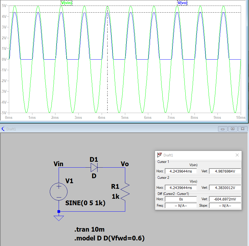
Figure 2: Circuit built for Task 1.2 in LTSpcie with a built in voltage of 0.6 V

Figure 3: Circuit built for Task 1.3 on a breadboard --> the built in voltage was around 0.7-0.8 V

Figure 4: Circuit built for Task 2.1 in LTSpice

Figure 5: Circuit built for Task 2.2 on a breadboard (this circuit is the same as in Figure 4)

Figure 6: Circuit built for Task 3.1 in LTSpice

Figure 7: Circuit built for Task 3.1 on a breadboard

Figure 7: Circuit built for Task 3.2 in LTSpcie modeling the Zener diode using a script.

Figure 8: Circuit built for Task 3.2 on a breadboard using a zener diode 1n530 (this circuit is the same as in Figure 7)
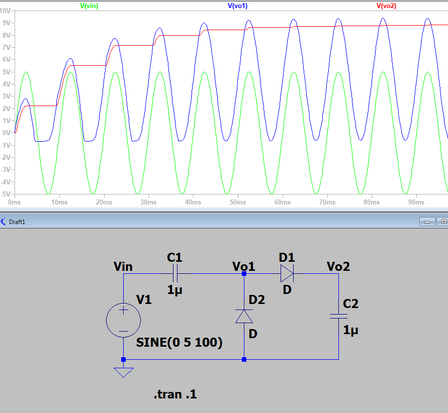
Figure 9: Circuit built for Task 4 in LTSpice

Figure 10: Circuit built for Task 4 on a breadboard
5. Discussion
The
results shown in Figure 1 for task 1.1 is that the circuit acts as a
half wave rectifier. When the input voltage is negative than the output
voltage is zero. When the input voltage is positive than the output
voltage attenuates but doesn't reach 5 V. The diode doesn't allow
current to flow through it when the input voltage is negative which is
why the output voltage is zero. But when the input voltage is postive
the diode does allow current to flow through it which is why we see an
output voltage. The built in voltage for the 1N5767 diode used in task
1.3 was 0.7 V.
For task 3.1 the circuit was acting as two half wave rectifiers, by
using both a forward biase and revers biased diode. These results are
shown in Figures 6 and 7. The simulated breakdown voltage for the 1N
3733 A diode matched the datasheets reported values and 5V.
For task 4 used a diode and a
capacitor to lift the circuit, and then went through a rectifier to
convert the voltage into a DC voltage value. This doubled the intitial
sine wave that was input into the system.