ENGR337 Lab 2020 Spring
Lab 4
Name: Jessica Shinkle
Email: jlshinkle@fortlewis.edu
1. Lab 3 Filters and Amplifiers
2. Introduction
The purpose of this lab is to amplify a small signal to the 0 - 5 V range.
3. Materials and Methods
In this lab there were 6
tasks. Task 1 and 2 were taking screen shots of a 500 mVpp, 1 Hz., with
an offset of 1 V. The only difference was that Task 2 used the AC
option in the channel's menu to remove the DC offset in the view. Task
3 was the same as Task 1 and 2 but a 3.3 V DC voltage was added. The DC
coupling and the AC coupling of the final signal were shown seperatly
on the function generator.
In Task 4 a low-pass filter was added to remove the 60 Hz noise. In
Task 5 a high-pass filter was added to the circuit to remove the DC
offset from the signal. In both of these tasks the resistor and
capacitor had to be hand calculated. Task 6 had three parts to it. In
part one a zenor diode to provide a 2 V reference voltage. The
resistors and capacitors had the same values as found in task 4 and 5.
A 3 V zener diode was used instead of a 2 V zener diode in this
section. A 741 Op Amp was used as the amplifier to provide the
gain. Part 2 in Task 6 was very similar to part 1. The only difference
was instead of sending the rails to 5 V they were sent to 10 V and a 5
V zener diode was used. Part 3 had a slightly different circuit.
The Op Amp that was used is a higher-end and has better quality.
4. Results

Figure 1: A circuit shown on the Function Generator (Task 1)
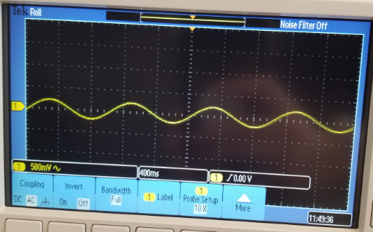
Figure 2: The same circuit shown in figure 1 but has the DC offset removed (Task 2)
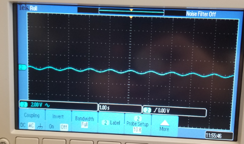
Figure 3: A circuit with a 3.3 V DC voltage added to it (Task 3)

Figure 4: Hand calculations for the low pass filter (Task 4)

Figure 5: The the circuit shown on the function generator (Task 4)
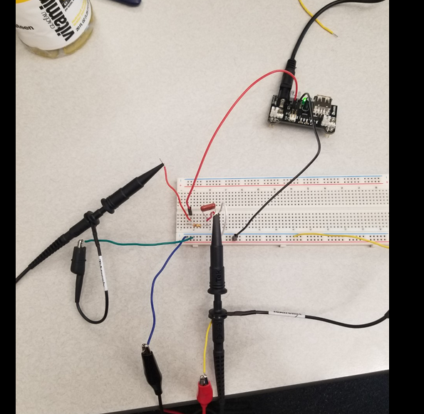
Figure 6: The circuit shown on the bread board of figure 5 (Task 4)

Figure 7: The hand calculations for the high pass filter (Task 5)

Figure 8: The circuit shown on the function generator (Task 5)
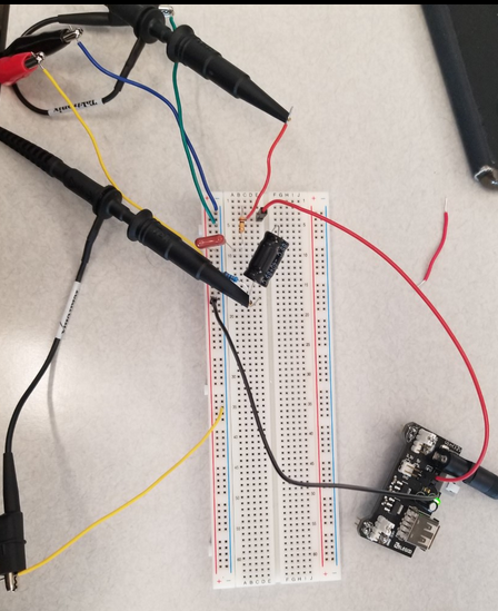
Figure 9: The circuit shown on the bread board (Task 5)

Figure 10: The circuit shown in part 1 on the function generator (Task 6)
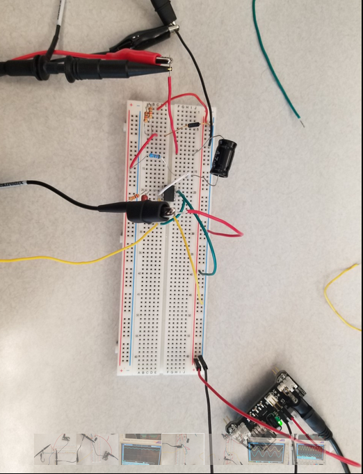
Figure 11: The circuit shown on a bread board of part 1 (Task 6)
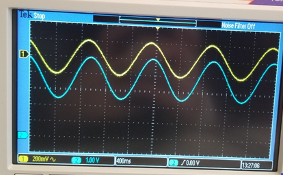
Figure 12: The circuit shown on the funtion generator of part 2 (Task 6)

Figure 13: The circuit shown on the bread board of part 2 (Task 6)

Figure 14: The circuit shown on the funtion generator of part 3 (Task 6)
5. Discussion
In Task 4 the difference between the input and output signals is that
the input is very fuzy due to the noise and the output is clean. In
Task 5 the input is the same as in Task 4 but the output is clean as
well as smaller. This lab was very helpful in understanding how op amps can amplify a circuit.