ENGR337 Lab 2018 Spring
Lab 2
Name: Jessica Shinkle
Email: jlshinkle@fortlewis.edu
1. Title: Lab 2: More Spice and the Compensated Probe
2. Introduction
This Lab is ment to continue increasing our knowledge on LTSpice and
learn how to use the function generator and the oscilloscope. We also
are practicing our knowledge on how to calculate the time delay by hand
for different circuits and how to size certain components of a circuit.
3. Materials and Methods (Do not simply list everything there, put them in a table if needed).
During
lab 2 LTSpice was utilized to simulate 9 circuits. The circuits in 1.1,
1.2, 3.1, and 3.2 were just made in LTSpice and not on a bread board.
In 1.3 and 2.1 the circuit were also built on a breadboard. A 1 k ohm
resistor and a 100 pF capacitor was used on the breadboard for 1.3. A
function generator was used to create a square wave and an oscilloscope
was used to probe the signal. The input/output was recorded For 2.1 a
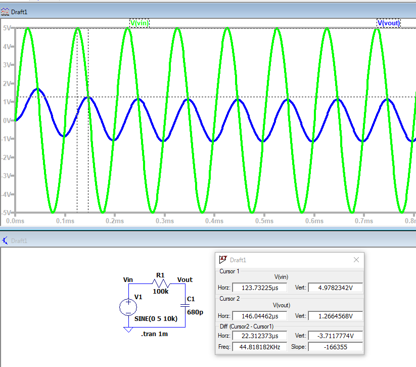
100 k ohm resistor and a 680 pF capacitor were used on the breadboard.
The function generator was used to create a sin wave and the
oscilloscope was used to probe the signal. The measurements taken from
the oscilloscope and the LTSpice were recorded and compared.
4. Results

Figure 1: LTSpice for the first circuit (1.1)
Figure 2: LTSpice for the second circuit (1.2 a)
Figure 3: LTSpce for the third circuit (1.2b)
Figure 4: LTSpice for the fourth circuit (1.2c)
Figure 5: LTSpice for the fifth circuit (1.2d)
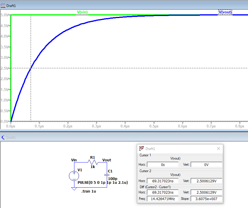
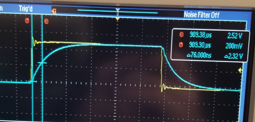
Figure 6: The time delay measured in LTSpice on the left and on the oscilloscope on the right (1.3)
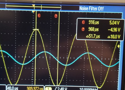
Figure 7: The time delay measured in LTSpice on the left and on the oscilloscope on the right (2.1)
Figure 8: The peak to peak measured for the input on the right and the output on the left (2.1)
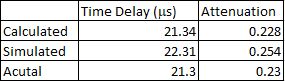
Figure 9: The table comparing the calculated, simylated, and measured time delays (2.1)
Figure 10: The LTSpice for the eighth circuit (3.1)
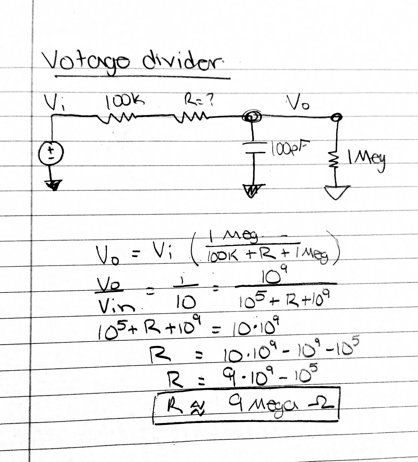
Figure 11: The calculations done by hand for the unknown resistor (3.1)
Figure 12: The LTSpice for the nineth circuit (3.2)
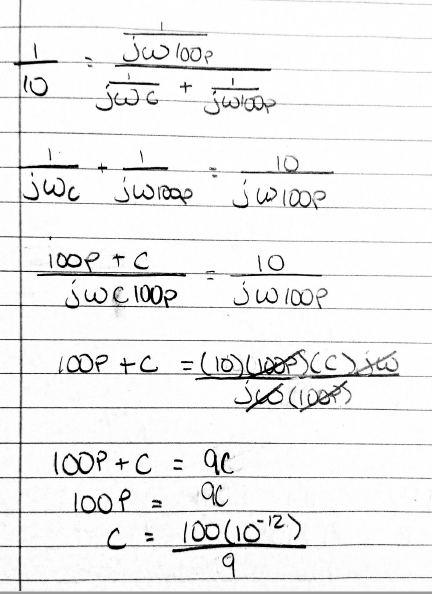
Figure 13: The calculation done by hand for the unkown capacitor (3.2)
5. Discussion
In
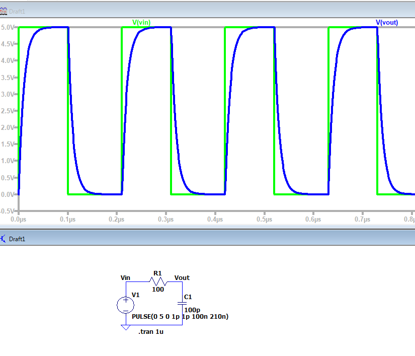
Figure 1 the frequency of the pulse function was too high to fully
charge the capacitor. In Figures 2 through 4 are almost the same
circuit just being adjusted to fully charge the capacitor. In Figure 2
the frequency is still too highe even though the voltage was reduced,
so the capacitor is not fully charging. In Figure 3 increasing the
duration that the pulse decreased the frequency allowing for more time
for the capacitor to reach full charge. In Figure 4 decreasing the size
of the capacitor from 100 pF to 10 pF decreased the time delay to fully
charge the capacitor. This allowed the capacitor to fully charge in to
210 ns time period. In Figure 5, the resistor was decreasing causing
the voltage drop across the voltage divider to decrease allowing a
higher voltage and current to the capacitor. In Figure 6 the measured
time delay measured
in LTSpice on the and on the oscilloscope were 74 ns and 76 ns,
respectively. In Figure 9 the table that has the calculated, measured,
and simulated values for the time delay and attenuation for the 2.1
circuit. These values are all really similiar.
For 3.1 Figures 10 and 11 show the LTSpice simulation and the hand
calculation to figure out what the value of the resistor was. The value
of the resistor was approximatley 9 Mega ohms. For 3.2 Figures 12 and
13 show the LTSpice simulation and the hand calculations to figure out
what the value of the capacitor was. The value of the capacitor was
approximatley 1.11 E-11.
The type of scope probe was simulated in LTSpice to finish the lab.
This was to see how the attenuation results from the internal
ressistance as well as the parasitic capacitance of the probe.