ENGR337 Lab 2020 Spring
Project - Final Chip Layout
Name: Donovan Birky
Email: dkbirky@fortlewis.edu
1. Title - Final Chip Layout
2. Introduction
The goal for this final project was to finish the IC chip layout, complete with op amp and inverter.
3. Materials and Methods
ElectricVLSI
was the software utilized for this final project. In previous labs, the
inverter was layed out along with the padframe (that included an
electrostatic discharge (ESD) ring). To finalize the IC chip, the
Op-Amp had to be created, and the final layout and schematic had to be
completed and pass both DRC and NCC checks.
The Op-Amp first required layout of the bias circuit which is used to
make sure that the Op-Amp adjusts the signal to the middle of its
range, ensuring that the maximum gain is able to be achieved. Once the
bias circuit is layed out, the rest of the Op-Amp can be layed out,
which is shown in Figure 5. The Op-Amp is made up of a differential
pair with a current mirror, followed by the gain stage, which uses
wider CMOS transistor technology to act as the signal gain for the
Op-Amp. The last addition to the Op-Amp design is the inclusion of a 10
pF capacitor, which helps increase the phase margin for the Op-Amp, in
the end making it more stable. Both the schematic and layout views for
both the bias circuit and Op-Amp are created in ElectricVLSI and
confirmed that they pass both DRC and NCC checks before continuing on
to the rest of the chip design.
Now the final layout can be completed. The ESD padframe is placed into
a new layout along with the Op-Amp and an inverter. The pins on the
padframe are exported according to Mosis specifications, and the Op-Amp
and inverter are wired to the padframe. Finally, the same is done in
the schematic view for the chip. Once the chip passes both DRC and NCC
checks, the final chip layout is complete.
4. Results

Figure 1. Inverter schematic and icon.
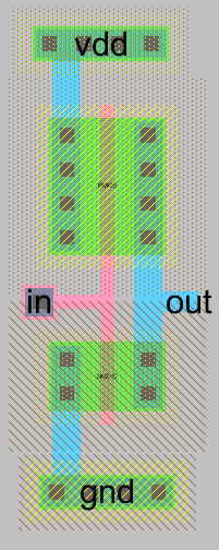
Figure 2. Inverter layout.
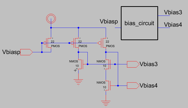
Figure 3. Bias circuit schematic and icon.

Figure 4. Bias circuit layout.
Figure 5. Op-Amp schematic and icon.
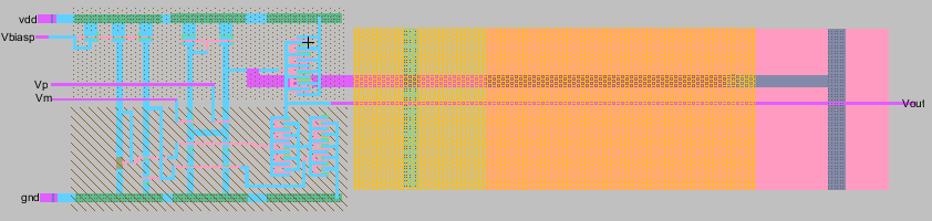
Figure 6. Op-Amp layout.
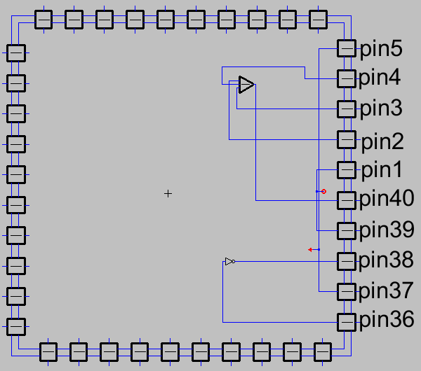
Figure 7. Final IC chip schematic.
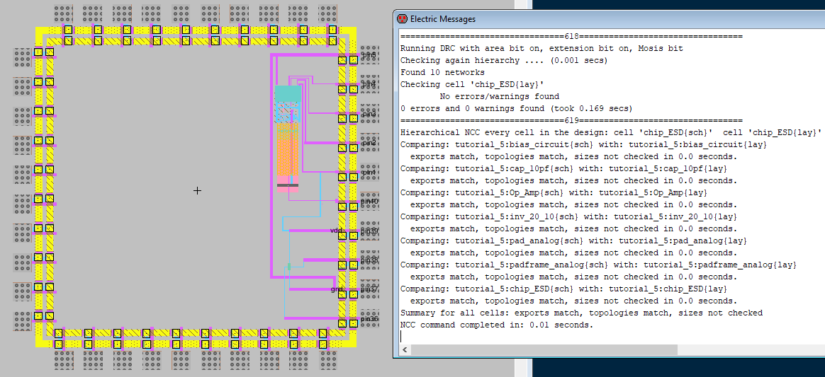
Figure 8. Final IC chip layout with confirmation of DRC and NCC checks
passed.
5. Discussion
Overall the final project was a success. Through
all of the tutorials the inverter, bias circuit, Op-Amp, and padframe
were all created successfully and finally assembled into the final IC
chip that is shown abobe in Figure 8. The final design passes both DRC
and NCC checks. There are still some final adjustments to be made if
the chip were to be fabricated (fixing well problems) but essentially
the chip is ready to be sent to be fabricated by Mosis, if and when the
C5 technology becomes available. The skills aquired in this project
were very unique, as IC design is something few undergrads get to
partake in, so this skill was very cool to learn. Thank you Dr. Li!