ENGR337 Lab 2020 Spring
Lab 9 Layout the Padframe
Name: Donovan Birky
Email: dkbirky@fortlewis.edu
1. Title - Layout the Padframe
2. Introduction
The goal for this lab was to layout the padframe for the chip with an electrostatic discharge (ESD) protection ring.
3. Materials and Methods
ElectricVLSI
software was utlized to layout the padframe of the chip. The first step
was to create both an Nwell/Pact and Pwell/Nact diodes. These two
diodes will be combined to prevent burnout on the chip due to ESD.
These diodes are wired up to a pad with a metal contact and passivation
layer, which is what the signals will be connected to once the chip is
fabricated. The ESD pad has six inputs/outputs, the two VDD
input/output, the two GND input/output, and the Analog connections.
These ports are exported, and the same ports are made in a
corresponding schematic. Now the pads are brought into a new layout,
and are made into a 10 by 10 frame by using the array feature in
ElectricVLSI. The pads are all connected, and finally is checked to
make sure it is DRC clean. A corresponding schematic is also made and
DRC/NCC checks are made to make sure the topologies match and the
layout/schematic will pass ERC.
4. Results
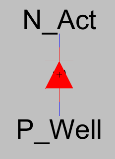
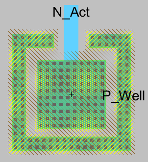
Figure 1. The Nact/Pwell diode schematic and layout.
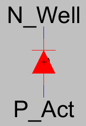

Figure 2. The Pact/Nwell diode schematic and layout.

Figure 3. The pad schematic.
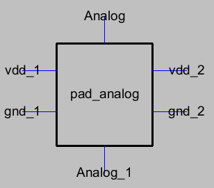
Figure 4. The pad icon.
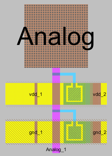
Figure 5. The pad layout.

Figure 6. The padframe schematic.
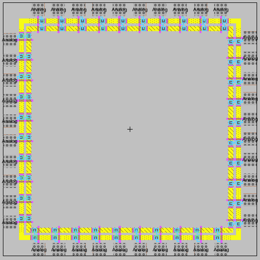
Figure 7. The padframe layout.
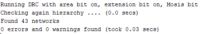
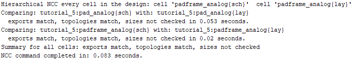
Figure 8. DRC and NCC notifications indicating the final design passes.
5. Discussion
Overall this lab was successful in laying out
the padframe for the chip. This padframe has the added feature of the
ESD protection ring, which will make the chip much less succeptible to
excess voltage failure. The wiring of the chip was the most difficult
part, mostly just tedious, but the final layout was successful and most
importantly DRC and NCC clean. This padframe will be utilized to layout
the rest of the chip for the final project.