ENGR337 Lab 2020 Spring
Lab 8 Layout an Inverter
Name: Donovan Birky
Email: dkbirky@fortlewis.edu
1. Title - Layout an Inverter
2. Introduction
The goal for this lab was to use ElectricVLSI to layout an inverter using PMOS and NMOS transistors.
3. Materials and Methods
ElectricVLSI
software was used to layout the transistors and LTSpice was used to
simulate the inverter configuration. The first step was to create the
inverter in the schematic, placing an NMOS and PMOS component into the
schematic. The drain of the PMOS is connected to the source of the
NMOS, and the two gates are connected. The source of the PMOS is the
power, and the drain of the NMOS is connected to ground. The gates act
as the input terminal, while the junction between the NMOS/PMOS drain
and source is the output terminal. This was all wired up in the
schematic view, then a simplified icon was created, which was simulated
using LTSpice.
The same process was utilized for the layout view. A PMOS and NMOS were
placed, along with two Pact and two Nact to act as the pins for the
source and drain of the two transistors. This was all wired up, and the
simplified layout view was utilized to simulate the inverter in
LTSpice.
4. Results
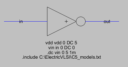
Figure 1. Inverter schemactic icon view.
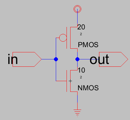
Figure 2. Inverter schematic.
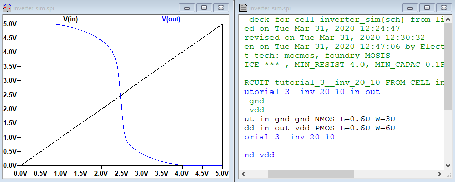
Figure 3. Inverter schematic simulation.
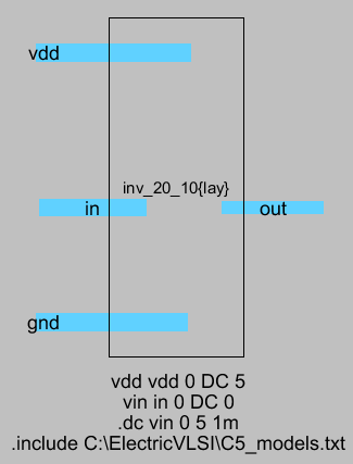
Figure 4. Inverter layout icon.
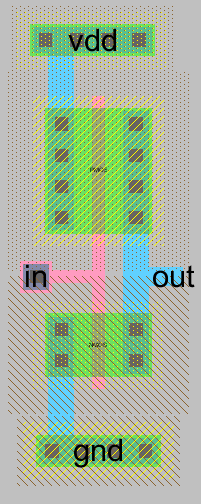
Figure 5. Inverter layout.
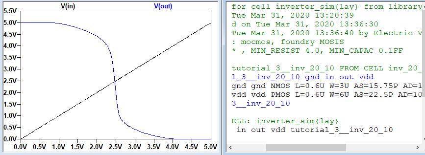
Figure 6. Inverter layout simulation.
5. Discussion
The inverter was successfully created using both
the schematic and layout views in ElectricVLSI, as is shown in the
simulations above, which acted in the way that was expected. Overall,
this lab utilized many of the skills layed out in the first two
tutorials, but was important to put them all together to create this
fundamental digital device. Having taken digital electronics, it was
cool to be able to actually layout the inverter that we talked a lot
about in that class.