ENGR337 Lab 2020 Spring
Lab 5 Rectifiers and DC Regulators
Name: Donovan Birky
Email: dkbirky@fortlewis.edu
1. Title - Rectifiers and DC Regulators
2. Introduction
The goal
for this lab was to better understand both rectifiers and DC
regulators, both circuits that require diodes for their operation. This
lab allowed us to simulate these circuits both in LTSpice and on the
breadboard and compare the results.
3. Materials and Methods
The first circuit to be designed was a half wave rectifier, which
required a 1k resisitor and a 1N 5767 diode. The circuit was powered up
with a 10 V Vpp sine wave with a 1k Hz frequency. This circuit was
cimulated in LTSpice as well as on the breadboard. The second circuit
added a 33u capacitor in parallel with the 1k resistor, which results
in a DC regulator. Again, the circuit was simulated and done on the
breadboard. The third circuit required two diodes, one forward biased,
while the other was reverse biased, in parallel and following a 1k
resistor circuit. The fourth circuit was a "clamp" voltage circuit
which required two 1N 3733A zener diodes, one forward biased and the
other reverse biased, in series with a 1k resistor. The last circuit
was a "voltage doubler" circuit, which requires two 1u capacitors, and
two 1N 5767 diodes, creating a lifted signal, followed by a rectifier
that will result in a final DC voltage double the original voltage.
4. Results

Figure 1. LTSpice simulation results for the half wave rectifier,
showing a built in voltage of 0.7V.

Figure 2. Breadboard simulation results for the half wave rectifier, showing a built in voltage of around 0.7-0.8V.

Figure 3. LTSpice simulation results for the half wave rectifier, now with a built in voltage of 0.6V.
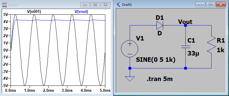
Figure 4. LTSpice simulation results for DC converter.

Figure 5. Breadboard simulation results for DC converter, also showing
the power supplies difficulty to swing 10 Vpp with the 33u cap.

Figure 6. LTSpice simulation for essentially two half wave rectifiers put together.

Figure 7. Breadboard simulation results for essentially two half wave rectifiers put together.

Figure 8. LTSpice simulation results for the "clamp" voltage circuit.

Figure 9. Breadboard simulation results for the "clamp" voltage circuit.
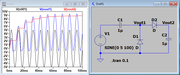
Figure 10. LTSpice simulation for the "voltage doubler" circuit.

Figure 11. Breadboard simulation results showing the intital vout of the "voltage doubler" circuit.
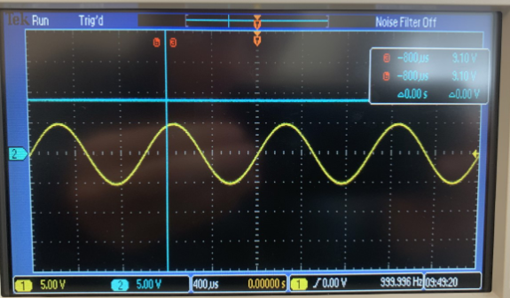
Figure 12. Breadboard simulation results showing the final vout of the "voltage doubler" circuit.
5. Discussion
The results for the first ciruit showed that this circuit acts as a
half wave rectifier. When the input voltage dips below zero, the diode
does not allow current to flow through it, resulting in zero volts.
When the input is positive, the diode does allow current to flow, but
it does not reach the full 5V input because of the built in voltage of
the diode. LTSpice showed that the ideal diode has a built in voltage
of 0.7V, which can be adjusted using .model. On the breadboard, it was
measured that the 1N
5767 diode has a built in voltage of around 0.7V as well. The next
circuit was a DC converter, which essentially uses a capacitor combined
with the recitfier to maintain a relatively constant DC voltage at 5V.
The breadboard simulation did not match simulation exactly, because the
power supply is not powerful enough to charge and discharge the large
33u capacitor.
The third circuit was essentially acting as two half wave rectifiers,
by using both a forward biased and reverse biased diode. The results
are shown in Figure 6 and 7. The fourth circuit was a "clamp" voltage
circuit which uses two zener diodes to essentially cut off the voltage
above and below the zener break down voltage of the diode. The 1N
3733A zener diode used proved to have a zener breakdown voltage of
around 5V according to simulation, which matched the datasheet's
reported values. The last circuit tested was the voltage doubler
circuit, which uses a diode and cap to lift the circuit (no current
passes through the reverse biased diode), then goes through a rectifier
to convert into a DC voltage value, essentially doubling the intitial
sine wave that was input into the system.