ENGR337 Lab 2020 Spring
Lab 2 More Spice and the Compensated Probe
Name: Donovan Birky
Email: dkbirky@fortlewis.edu
1. Title - More Spice and the Compensated Probe
2. Introduction
The goal
for this lab was to continue familiarizing ourselves with running
simulation in LTSpice, performine AC analysis using the oscilloscope,
and understanding the mechanisms behind the compensated scope probes.
3. Materials and Methods
This lab required LTSpice to run
simulations on the first five circuits, adjusting various parameters to
see what allowed the capacitor in the circuit to reach the complete
voltage supplied. Next a signal generator was used to supply a 5V
square wave to an RC circuit built on a breadboard using a 1k resistor
and a 100pF capacitor. An oscilloscope was used to measure both the
input and output signal, measuring for the time delay in the circuit.
The next circuit required a 100k resistor and a 680p capacitor and was
supplied with a 5v/-5v sine wave. Again, the oscilloscope was used to
mesaure the signal attenuation and time delay. This circuit was also
simulated, as well as hand calculated, so that the predicted and actual
time delay and attenuation could be compared. Finally, a circuit was
simulated in LTSpice to show the internal circuit of the compensated
probe and show how the internal resistance and parasitic capacitance
attenuates the measured signal.
4. Results

Figure 1. First circuit simulation.
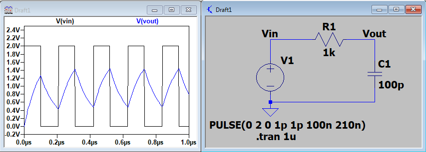
Figure 2. Second circuit simulation.
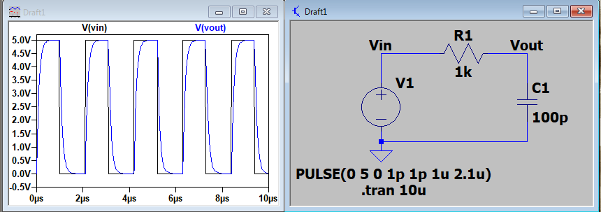
Figure 3. Third circuit simulation.
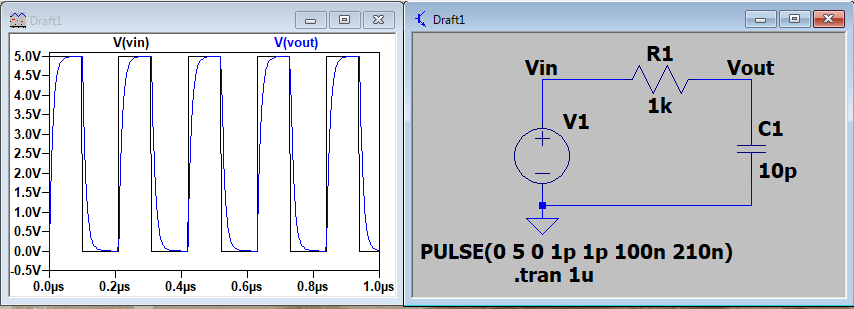
Figure 4. Fourth circuit simulation.

Figure 5. Fifth circuit simulation.

Figure 6. The time delay for the RC circuit built on the breadboard.
Table 1. Results for attenuation and time delay for the RC circuit.
|
Attenuation
|
Time Delay
|
Calculation
|
0.23
|
20µs
|
Simulation
|
0.23
|
20.9µs |
Oscilloscope
|
0.23
|
21.2µs |
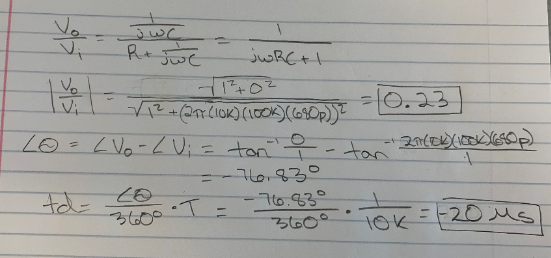
Figure 7. Calculation for the attenuation and time delay of the RC circuit.

Figure 8. Simulation finding the time delay of the RC circuit. Similar method used for finding attenuation.
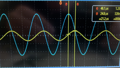
Figure 9. Finding time delay on the oscilloscope. Similar method used for finding attenuation.
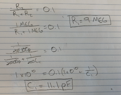
Figure 10. Calculations for finding the proper resistance and capacitance for 10x attenuation.

Figure 11. The compensated probe circuit with 10x DC attenuation.
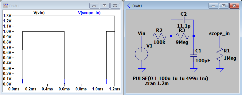
Figure 12. The compensated probe circuit with 10x DC and AC
attenuation.

Figure 13. Using the oscilloscope on 1x.
5. Discussion
The first few RC circuits simulated in LTSpice demonstrated how various
parameters can be changed to maximize/minimize the capacitors ability
to fully charge/discharge. Figure 1 shows the time delay being too
large, not allowing the cap to fully charge/discharge. Figure 2 shows
that a change in the amplitude does nothing for helping this fact.
Figure 3 shows that a change in the frequency of the signal, making it
larger, allows the capacitor to fully charge and discharge. Figure 4
and Figure 5 show that this can also be done by either decreasing the
capacitance of the capacitor (making it easier to charge) or increasing
the resistance (less current flowing).
The RC circuit results shown in Figure 6 show a time delay of 88ns for
the square wave input. Next a sine wave input was used with a frequency
of 10k Hz. The attenuation and time delay were calculated, simulated, and
analyzed on the breadboard, and the results are reported in Table 1.
The results matched up very well between all three methods.
Lastly, the compensated probe was simulated in LTSpice to see how the
attenuation results from the internal resistance as well as the
parasitic capacitance of the probe. The proper resistance and
capacitance were found by treating them individually as voltage
dividers attenuating the signal by 10x. These calculations are shown in
Figure 10 and the simulations are shown in Figures 11 and 12. Figure 13
shows the use of the probe on the 1x setting (despite inputing a 5V
sine wave the result is only around 150mV).