ENGR337 Lab 2020 Spring
Lab 9: Layout the Padframe
(Tutorial 4 in Tutorial Series)
Name: Audra Benally
Email: albenally1@fortlewis.edu
1. Title: Layout the Padframe
2. Introduction: In this study, I followed another tutorial and got
even closer to finishing my chip in Electric VLSI. This tutorial showed
me how to create an electrostatic discharge (ESD) frome that will
protect the chip pins.
3. Materials and Methods:
Materials:
- Computer with ElectricVLSI software
- Computer Mouse
Methods:
The first step to making the padframe of the chip
was to create the diodes. I made a nAct/pWell diode as well as a
pAct/nWell diode. The two diodes were connected to an analog pad with
metal for connecting to the outside and a metal to connect to the inner
chip parts. The diodes were set up in a way to prevent excessive
voltage discharges which may damage the inner chip layout. Once the pad
was created and checked, the pads were placed on a 5000 by 5000 frame
under the layout of the padframe. The pads were placed in an array of
10 pads across the lengths of the frame; so there were a total of 40
pads around the entire perimeter of the frame. Each pads' vcc pins and
gnd pins were connected to one another on the metal 3 layer to create
two rings: one vcc ring and one gnd ring. The metal 3 contacts were
meticulously placed to appease the NCC check. After the layout was
created the schematic was made in the same manner using the icons.
4. Results:
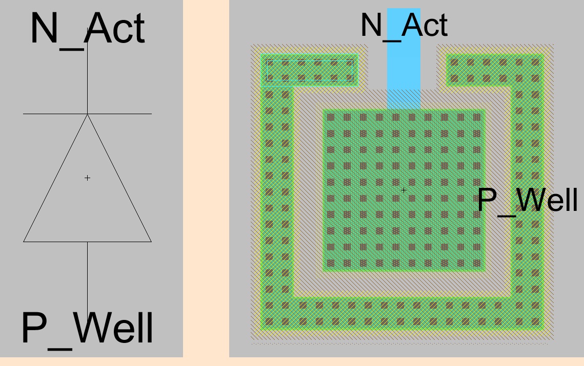
Figure 1. nAct / pWell diode schematic and layout.
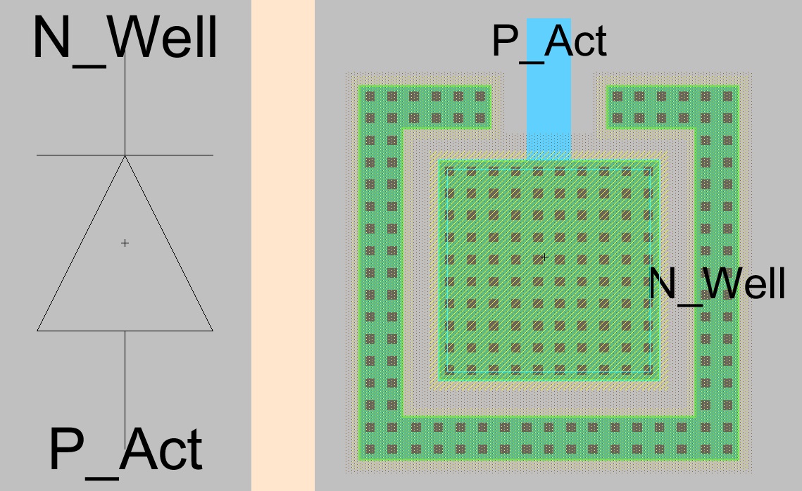
Figure 2. nWell / pAct diode schematic and layout
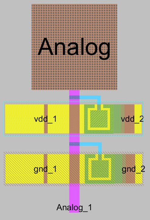
Figure 3. Analog pad layout with 6 pins labeled.
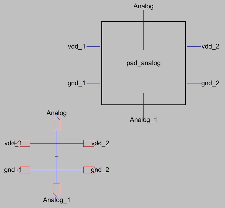
Figure 4.
Analog schematic and icon with the 6 pins from the layout above labeled.
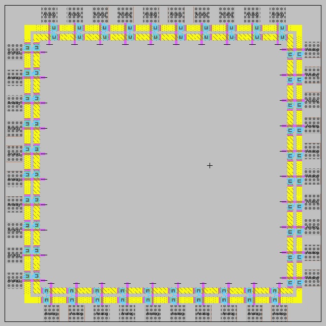
Figure 5.
Analog padframe layout with all 40 pads connected around the 5000x5000
frame.
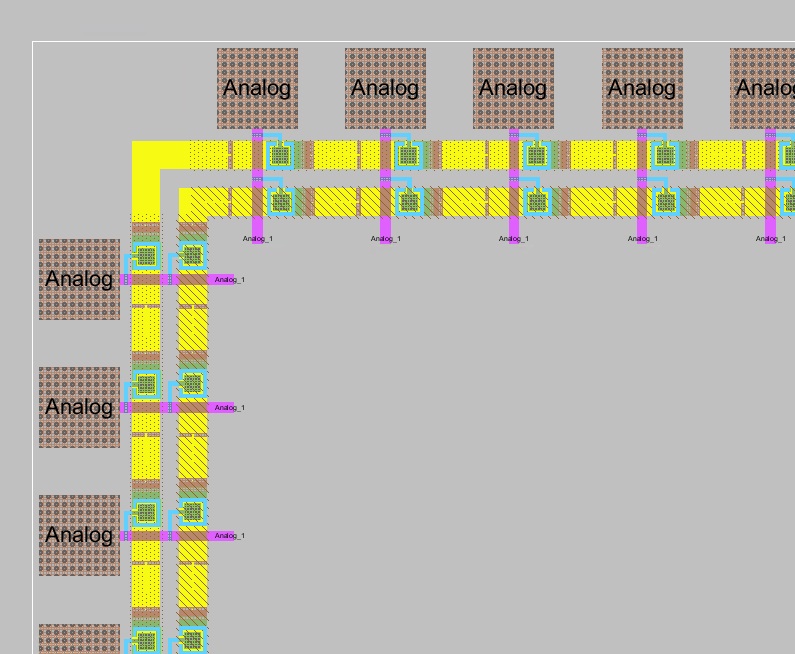
Figure 6.
Close up of the top left corner of the analog padframe layout.
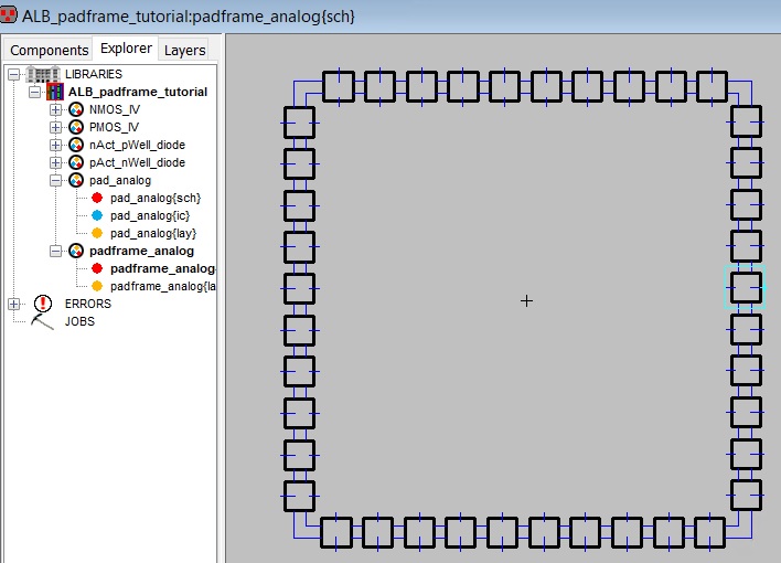
Figure 7. Analog padframe schematic view.
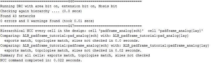
Figure 8.
Successful NCC and DRC checks for the analog padframe layout and
schematic.
5. Discussion:
This was one of the more tedious parts of these
tutorials; I still enjoyed it though. I am a perfectionist and it was
really satisfying making everything straight and orderly and not just
because I want to. The components went together well without much
issue. The only thing that was frustrating was the pure n-well-node and
p-well-node layers that would not let me click them. I found out it was
because "Easy to select" box was unchecked. Other than that, this was a
great lab with positive results.