ENGR337 Lab 2020 Spring
Lab 8: Layout an Inverter
(Tutorial 3 in Tutorial Series)
Name: Audra Benally
Email: albenally1@fortlewis.edu
1. Title: Tutorial 3: Layout an Inverter
2. Introduction: The goal for this lab is to create an inverter
using several different methods. The inverter was made using schematics
as well as layouts in the ElectricVLSI software.
3. Materials and Methods:
Materials:
- Computer with LTSpice
- Computer with ElectricVLSI
- Computer mouse - NOT a laptop touchpad
Methods: Follow the online tutorial to learn how to make
an inverter with NMOS and PMOS transistors. First, the schematic
inverter was made using the schematatic form of the previously made
NMOS and PMOS transistors. The transistors were edited and connected to
form the inverter. A symbol for ground and VDD power were added to the
appropriate positions. The gates were connected and labeled "in". The
PMOS dran pin was wired to the NMOS source pin and labeled "out". An
icon was added to the mix and recreated to look like the well-known
inverter symbol. Then the icon was put in its own cell and labeled for
spice simulation. LTSpice was used to simulate the Vin / Vout graph.
After the schematic was done, a
separate layout was made where the inverter was built from the ground
up. The separate p+/n+/pAct/nAct/pWell/nWell components were all laid
out and connected with a PMOS transistor on top and an NMOS transistor
on the bottom. The layout was appropriately labeled for simulation then
simulated in LTSpice.
4. Results:
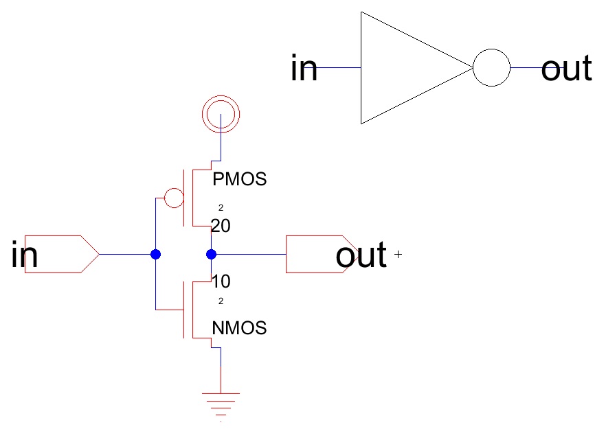
Figure 1.
Inverter schematic with size 20 (width) PMOS and size 10 (width) NMOS.
The icon is shown on the top right.
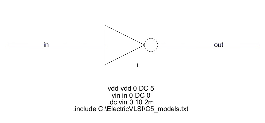
Figure 2. The
"in" and "out" labeled simulation for the schematic layout. I changed
the .dc code to better show the output in the simulation.

Figure 3. The
simulated output of V(in) and V(out) in LTSpice. The inverter switch
point (4.5V) is much higher than expected (2.5V).

Figure 4. The
schematic "grount-up" created inverter with a PMOS width of 20 and NMOS
width of 10. Both lengths are 2.
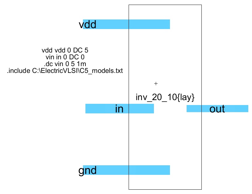
Figure 5. The simulation ready layout inverter with exported "vdd" and "gnd" pins and labeled in and out arcs.
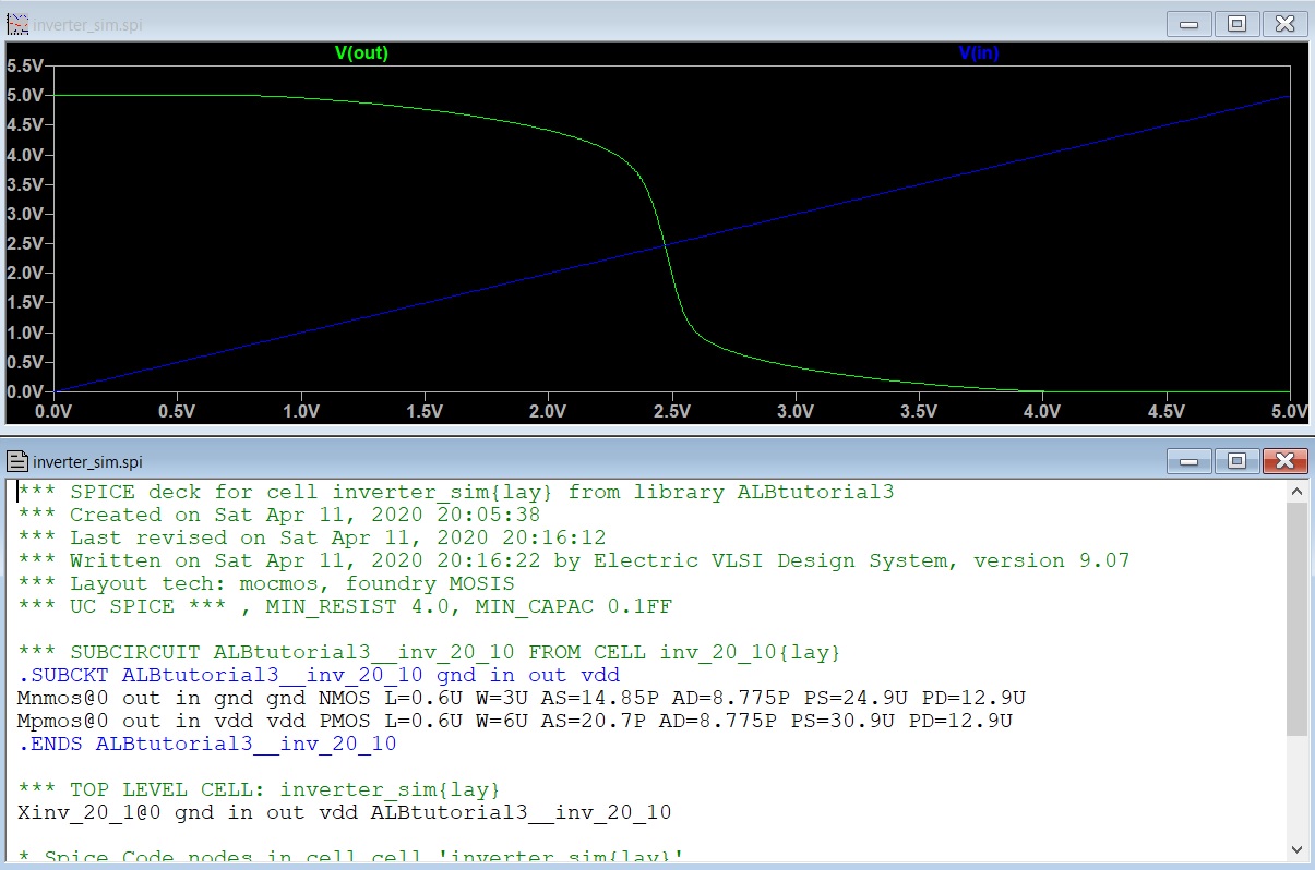
Figure 6. The LTSpice simulation of the layout form of the inverter. Output behaved as expected.
5. Discussion:
The inverter for the schematic
view was not quite as expected (see Figure 3). The switching point of
the inverter is much higher than 2.5V (it was measured at about 4.5V),
in fact I rewrote the code to go from 0 to 10 so I could better show
the switching point. I am unsure what I had done wrong. I redid the
schematic really quick and had a much worse output that didn't resemble
the expected output at all. The schematic version of the inverter
worked perfectly though. There were no issues with the schematic
version, I even found myself zipping through the instruction easier
because I was more familiar with the software. It was exciting.