ENGR337 Lab 2020 Spring
Lab 7: Layout an NMOS and PMOS in ElectricVLSI
(Tutorial 2 in Tutorial Series)
Name: Audra Benally
Email: albenally1@fortlewis.edu
1. Title: MOSFETs and IV Curves
2. Introduction: In this study we follow another tutorial in the
tutorial series. This tutorial shows how to create a NMOS and PMOS
transistors in Electric VLSI. The goal of the entire tutorial series is
to become familiar with the Electric VLSI software for circuit layout
and simulation.
3. Materials and Methods:
Materials:
- Computer with Electic VLSI software
- LTSpice software on the same computer
Methods:
This study showed how to change a schematic to other certain forms, in
this case a 4-pin NMOS and PMOS were used as opposed to the given 3-pin
transistors. The 4-pin transistors were used to get access to the
device's body so it could be connected correctly in each transistor.
The layouts were much more complicated for transistors than with
regular resistors. The different connector components of the transistor
were available and used to construct the transistors: pWell, nWell,
pAct, and nAct. A metal contact was used to show on the chip where the
gate would be connected. Once the transistors were assembled, the
circuit was supposed to be simulated in LTSpice. I was unable to get
the simulation to run. I was also sick during the lab so I didn't
finish my lab until a later date which I was unable to get help.
4. Results:
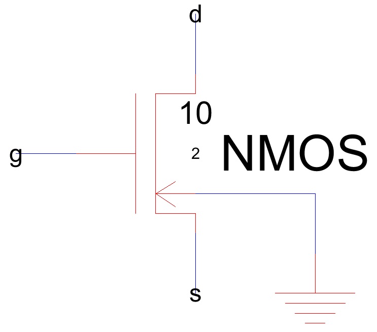
Figure 1.
Completed NMOS schematic layout with exported pins and grounded body
pin.

Figure 2. Completed NMOS layout with LTSpice code on bottom left.
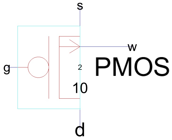
Figure 3.
Complete PMOS schematic with exported pins and body connected to "w".
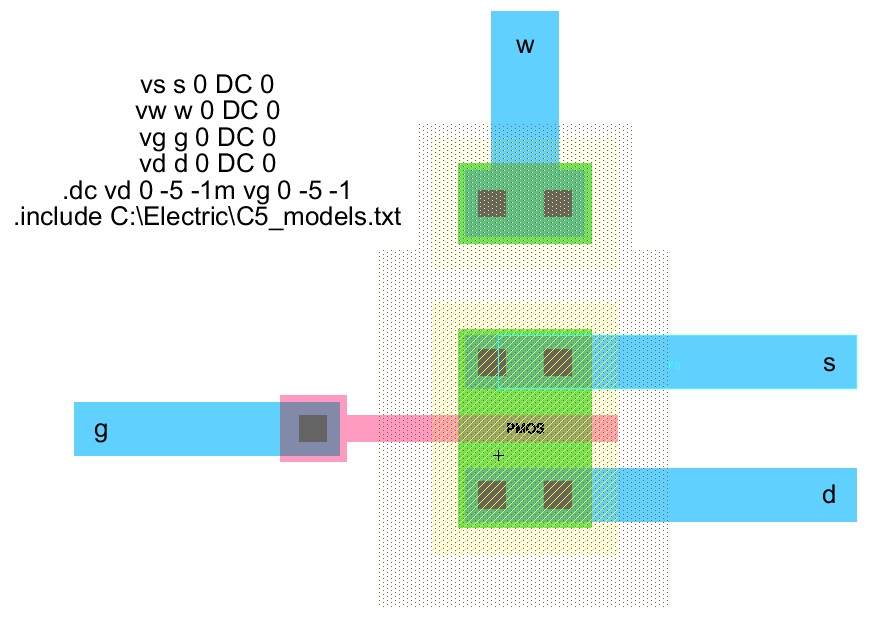
Figure 4.
First completed PMOS layout. This circuit was unable to run in LTSpice.
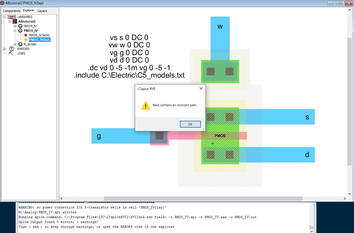
Figure 5. Window that pops up when "Write Spice Deck" was clicked.
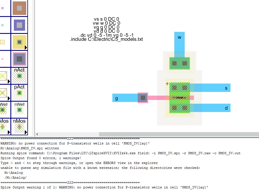
Figure 6. The
same errors occurred after the PMOS layout was reassembled and
properties from beginning of tutorial 1 were redone.
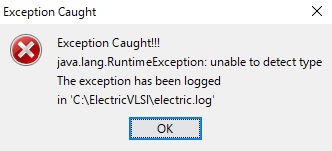
Figure 7.
Error window that popped up after trying to choose the specific PMOS
layout to run with spice.
5. Discussion:
In this lab, I was able to get the layout and
schematics of the NMOS and PMOS with ElectricVLSI. I was unable,
however, to run the simulation on LTSpice. I continuously got an error
while trying to run the PMOS layout. The warning given says there
are no power connection for the P-transistor wells but there shouldn't
need to be connections. That property looks to be associated with a box
that was unchecked during the well check properties.
I was unsure what to do about my problem so I did a couple things: 1. I
rechecked the file path for the LTSpice program, 2. I rebuilt the PMOS
transistor from scratch - following the tutorial again, 3. I went back
to tutorial 1 to redo all the property changes, and 4. I closed and
reopened the program. After trying these steps I still was unable to
get the simulation to run (see Figure 6 and 7) so I decided to give up
and maybe try again when I have access to assistance.