4. Results:
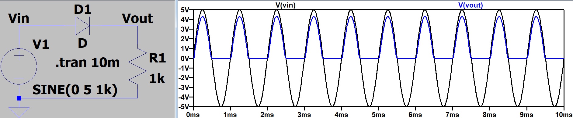
Figure 1. Task 1 LTSpice simulation of a diode connected in forward bias in series with a 1k-Ohm resistor.
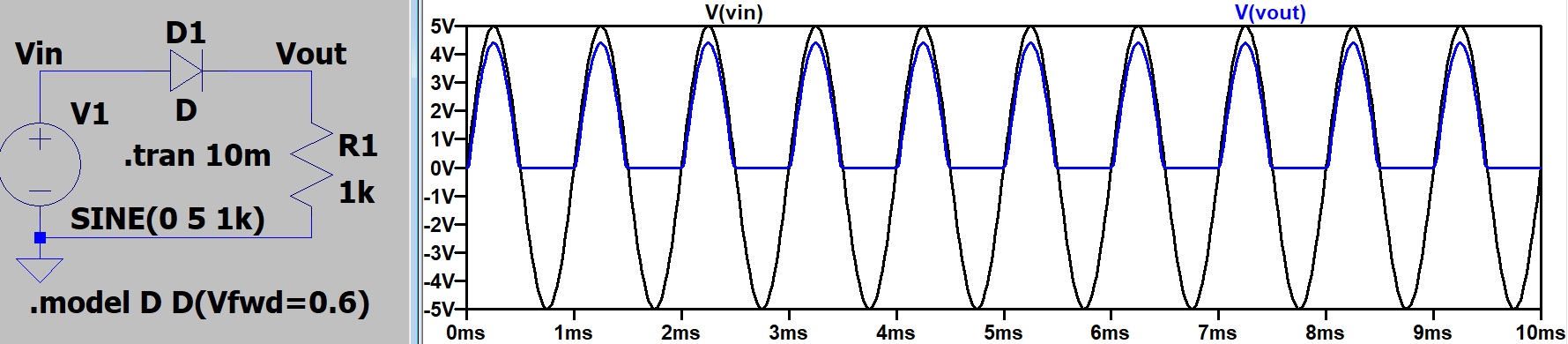
Figure 2. Task 1 simulated circuit after the built-in potential was changed to 0.6V

Figure 3. Task 1 circuit on the oscilloscope. The scales are different (2V and 5V) so the blue (Vout) signal is smaller than it really is.
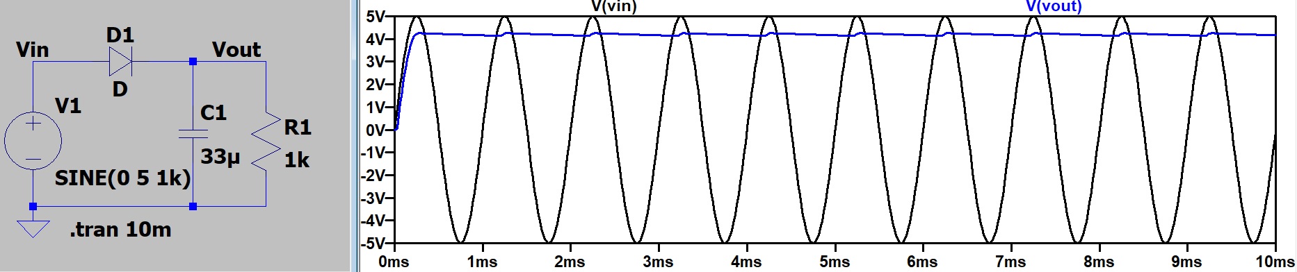
Figure 4. Task 2 LTSPice simulation.

Figure 4. Task 2 circuit V input (yellow) and V output (blue). The scales were also different in this picture so Vout is lower than it really was.

Figure 5. Task 3 part 1 LTSpice simulation, the diodes connected in opposite biases in parellel with the Vin are capping the input wave in the positive and negative ranges.

Figure 6. Task 3 part 1 circuit voltage input (yellow) and output (blue). The scales were different in this picture as well.
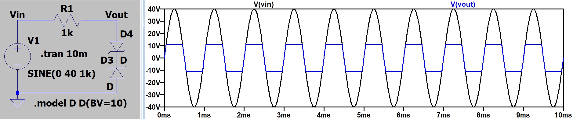
Figure 7. Task 3 part 2 LTSpice simulation of Zener diodes connected in a way that caps the voltage input at a specified voltage.

Figure 8. Task 3 part 2 Vout is "clamping" Vin, a method used to protect circuits against high voltages.
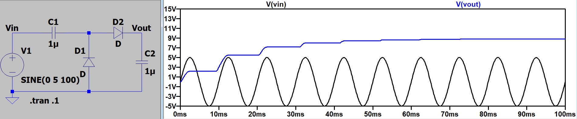
Figure 9. Task 4 LTSpice simulation AC to DC voltage.
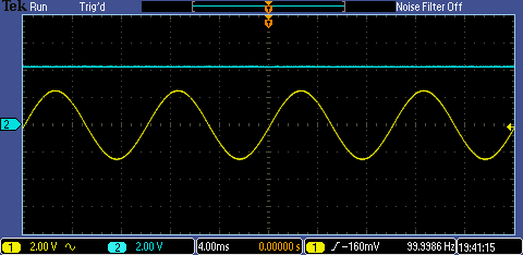
Figure 10. Task 4 circuit DC Vout signal
5. Discussion
In this experiment, we were able to recreate the results of the simulation in every task. It wasn't until the report was being put together that I realized we forgot to make the scale the same in several figures. This explains some confusion during the experiment. The only unclear result at the time was in Task 4 when we powered up the circuit it immediately shot up above the analog Vin signal. When the circuit was disconnected the Vout slowly went down as the capacitors discharged which made the results clearer as to what happened.