4. Results:

Figure 1. Task 1, function generator used to generate a wave on the oscilloscope.

Figure 2. Task 2, DC offset removed by pushing the left button under "Coupling"

Figure 3. Task 3, DC module added noise to the original wave.
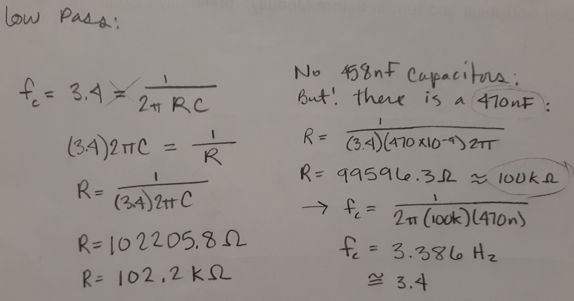
Figure 4. Low pass filter calculations. The original suggested capacitor was unavailable so there are recalculations for a different capacitor that would provide the same cutoff frequency.

Figure 5. Task 4, Low pass filter added. Vin is in yellow and Vout is blue.

Figure 6. Calculations for the resistance value for the high pass filter with a cutoff frequency of 0.5Hz.

Figure 7. Task 5, High pass filter added to remove DC offset. Notice the "Coupling" is set to DC and the Vout wave is still present.

Figure 8. Task 6, set up of the circuit that was supposed to add gain. Unfortunately our group wasn't able to get the circuit to work.

Figure 9. Vout was not acting as it should have. The issues of this reaction was unknown.

Figure 10. The High pass filter wasn't working the way it was before, the Vout signal is far above the Vin and not seen when "Coupling" is set to DC.
5. Discussion
In this lab, the first 5 tasks went smoothly with very little complications. The low pass filter worked correctly by eliminating the noise and allowing the 1Hz source through. The high pass filter worked by offsetting the DC voltage and appearing on the screen when "Coupling" was set to "DC". The 6th task though went unfinished because our Vout wasn't reacting the way it should have. My partner check and rechecked my wiring without finding any issue. We changed out all the capacitors and the op amp in case they were faulty but there wasn't any change in the flat Vout signal. We were told to check the voltages of the different components and everything looked like it was working correctly. I admit I don't have enough experience with actual hardwire so I may have missed something that was giving odd readings. Perhaps we wired the voltage source incorrectly? In the end, we were not able to figure out the problem before the end of the lab session.