Lab 3
Filters and Amplifiers
1. Introduction
The purpose of this lab is very simple: ampilfy a small signal (500
mVpp, 1 Hz, 1 V DC offset) to the 0-5 V range.
We prefer the 0-5 V range is
beacuse we assume the power supply for the
entire system is 5 V. The dynamic range of the Analog-Digital Converter
(ADC) is 0-5V.
2. Experiments and tasks
Task 1: Generate the
signal shown in Fig. 1 from a function generator and display it
on the scope. Make a screenshot of the view for your report.
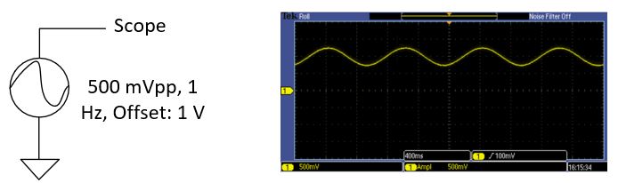
Fig. 1
Task 2:
Use the 'AC' option in the channel's menu to remove the DC offset in
the view. Make a screenshot of the view for your report.
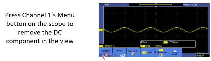
Fig. 2
Task 3:
Add a 3.3 V DC voltage from the 3.3V-5V DC module to the
sinewave you used above. Show the DC coupling (not shown in Fig. 4) and
the AC coupling of the final signal separately.
Make a screenshot of the view for your report.
The 3.3-5V DC modlue (ignore
the wire connections in the following figure):
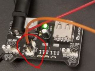
Fig. 3
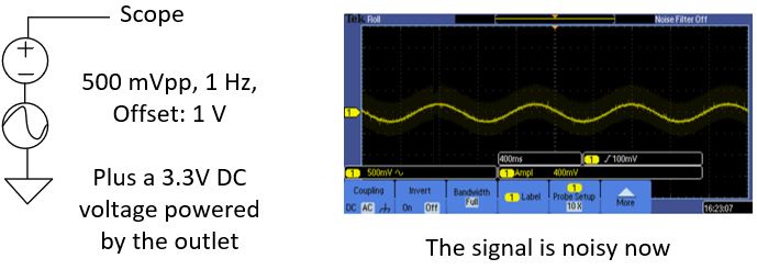
Fig. 4
You will notice that the
sinvewave looks a little more noisy than the
one doesn't have anything added to the sinewave. The 60 Hz noise comes
from the outlet. The 3.3-5V module is powered up by the outlet and this
noisy is being added to the circuit in series.
Task 4:
Add a Low-Pass Filter to remove the 60 Hz noise. Display the
input and the output at the same time and identify the differences of
the input and the output signals. Make a screenshot of the view for
your report.
If fc is designed to be 3.4
Hz, C=458 nF, what is the appropriate R?
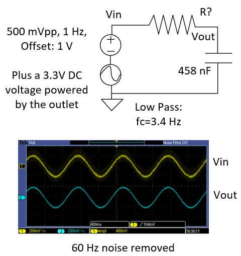
Fig. 5
Task 5:
Add a High-Pass Filter at the end to remove the DC offset from the
signal. Display the input and
the output at the same time and identify the differences of the input
and the output signals. Make a screenshot of the view for your report.
If fc is designed to be 0.5
Hz, C=4.7 uF, what is the appropriate R?
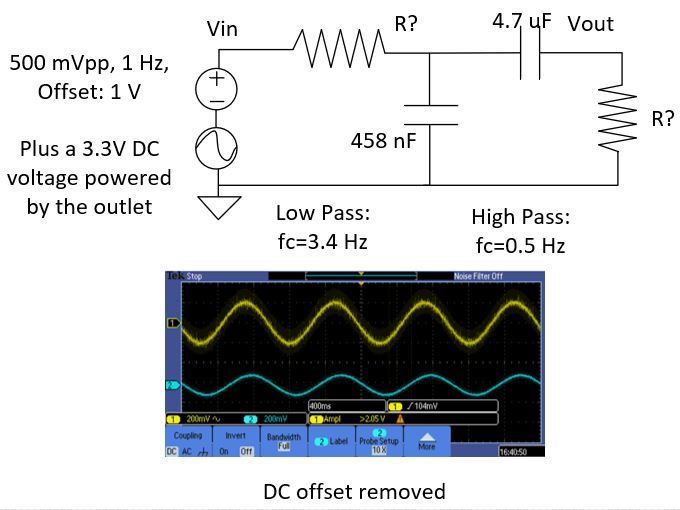
Fig. 6
However, the signal is being attenuated. We need some gain to be
applied to the signal so we can utilize the whole dynamic range of the
0-5 V ADC.
Task 6: Repeat the results in Fig. 9, Fig. 11, and Fig. 13. Make screenshots of the results for your report.
Let's add some gain to the
signal. Use the 741 Op Amp
(low quality and low cost) as the amplifier.
Add a 2 V DC offset to the signal from a 'reference voltage'. The
reference voltage is provided by a 680 ohm resistor and a 2 V zener
diode (1N4370 Zener). If you do not have it, you can use some
alternative ones, such as the 3 V ones.
The typical V-I curse for the
Zener diodes looks like the following figure. An Reversed Biased zener
diode can stablize the voltage at a specific level. The following one
shows the voltage is stablized at 3.4 V for reverse biasing.
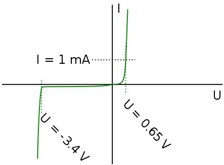
Fig. 7
Use a 1N4370 zener diode to
provide a 2 V reference voltage. You may use an alternative one to
stablize it at 3 V too. Use the same R's and C's in your passive filter
for the following circuit. Use a 741 Op Amp as the amplifier to provide
the gain.
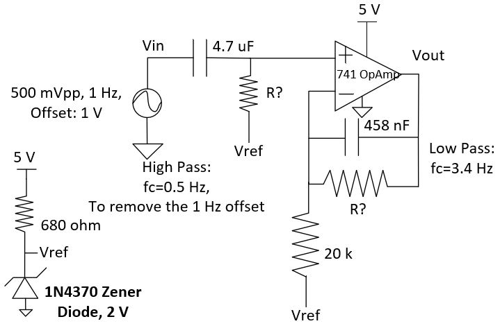
Fig. 8
However, the bottom of the
output signal is cut off.
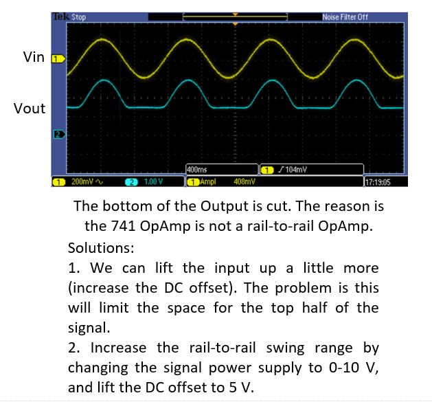
Fig. 9
The 741 is a low-cost and
fair quality Op Amp, it is not a rail-to-rail Op Amp and it is
amplifying the DC tiny difference between the two inputs and causing a
large DC offset at the output. We can fix it by inceasing the
rail-to-rail power supply to 10 V and lift the signal to 5 V as the DC
reference (offset) voltage.
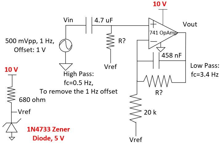
Fig. 10
Now it works for the same
signal:
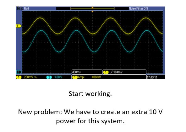
Fig. 11
However, you have to provide
an extra 10 V power in your system to amplify/filter the signal. If we
only have 5 V available in the system, we have to use a higher-end and
better quality Op Amp - the instrument amplifier.
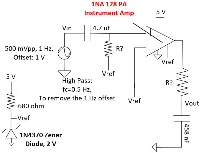
Fig. 12
The output is shown below.
Keep in mind, change the output coupling mode to DC to verify that your
signal is being amplified within the 0-5 V range without any
distortion.
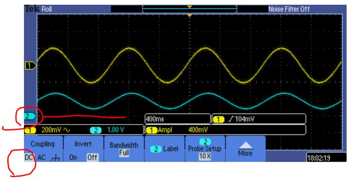
Fig. 13
The final circuits look like
this:
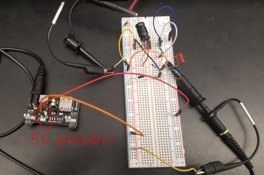
Fig. 14
The end of the lab