ENGR201 Lab 2018
Fall
Lab
8 Inductors and Boost Converters.
Outcome
of this lab:
1.
Practice on soldering.
2. Observe and analyze the voltage waveforms obtained when
charging/discharging a inductor through a resistor.
3. Measure the (magnitude of) the frequency response of an RL low-pass
filter and high-pass filter.
4. Build a
voltage booster using inductors, resistors, diodes, and capacitors.
Instructions:
Watch the video for more instructions.
PDF Notes
An
inductor is also a passive element designed to store energy but in its
magnetic field. They are widely used in power supplies, transformers,
radios, TVs, electric motors and so on. Inductors are unique in that
they can be magnetically coupled such that
a time-varying current in one will cause a voltage to be generated in a
second inductor in close proximity. This ‘mutual inductance’ is the
basis for the electrical transformer that is ubiquitous in the electric
power industry. Transformers, with their impedance transforming
property are also useful in electronic circuits over almost the entire
frequency spectrum.
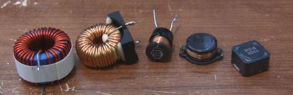
Also, inductors
are usually
formed into a cylindrical coil with many turns of conducting wire to
enhance the inductive effect. Various inductors and
transformers are shown in Fig. 1.
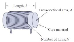
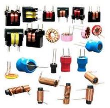
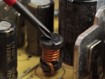
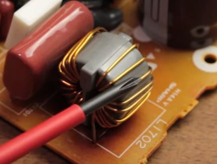
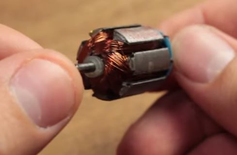
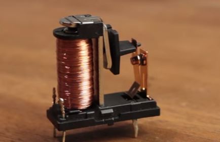
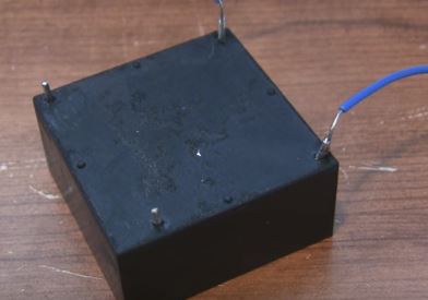
Fig. 1 Inductors
You can find
coils (inductors) very often in different situations:
When current
flows through a wire, it creates a magnetic field around it, more
current, bigger field.
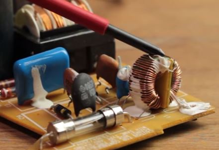
To increase the
magnetic field created by current, you can make a coil out of a wire,
and put a metal core inside the coil.
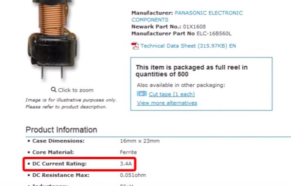
An inductor will
have its maximum DC current limit. Too much DC current will burn the
inductor.
The can be in
nanohenry, microhenry, and milihenry range:
Nanohenry range
inductor:
Microhenry range
inductors:
Milihenry range
inductor: (huge)
Tasks:
1. Build the
following circuit in LTSpice and solder it on a PCB board.
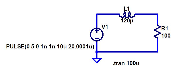
What is the delay of the Vout compared to Vin? Compare your hand-calculation, simulation, and measurement on a Prototype PCB.
2. Change the
input to a sinewave as shown in the following figure.
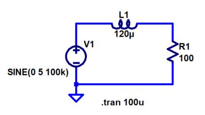
Why
the output is attenuated? Can you explain this qualitatively?
What if you decrease the frequency? Does the output increase or
decrease? Why? Explain this qualitatively.
What
if you increase the frequency? Does the output increase or decrease?
Why? Explain this qualitatively.
In
task 1, you already had this circuit on a prototype PCB, so change the frequency of the
input signal to a sinewave and show at which frequency (roughly), the
signal starts being attenuated?
3. Build
the following circuit in LTSpice:
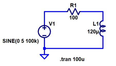
Why
the output is attenuated? Can you explain this qualitatively?
What if you decrease the frequency? Does the output increase or
decrease? Why? Explain this qualitatively.
What
if you increase the frequency? Does the output increase or decrease?
Why? Explain this qualitatively.
Build this circuit on a prototype PCB, show at which frequency (roughly), the
signal starts being attenuated?
4. Boost
converters:
Let's make
something practical out of inductors and capacitors: (Super
useful for DC-DC converters)
A boost
converter (step-up converter) is a DC-to-DC power converter
that steps up voltage (while stepping down current) from its input
(supply) to its output (load). It is a class of switched-mode power
supply (SMPS) containing at least two semiconductors (a diode and a
transistor) and at least one energy storage element: a capacitor,
inductor, or the two in combination.
The basic
circuit model for a boost converter:
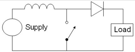
Because
the switch is turning on and off so fast, the inductors magnetic field
never fully collapses, so when the switch is opened again, this causes
a higher voltage on the inductor as it adds to the magnetic field.
Watch the
animation for better understanding of this circuit.
(the video is re-capped from an Youtube Channel at here).
Let's build a Boost Converter in LTSpice!!!
Try the following circuit by yourself in LTSpice:
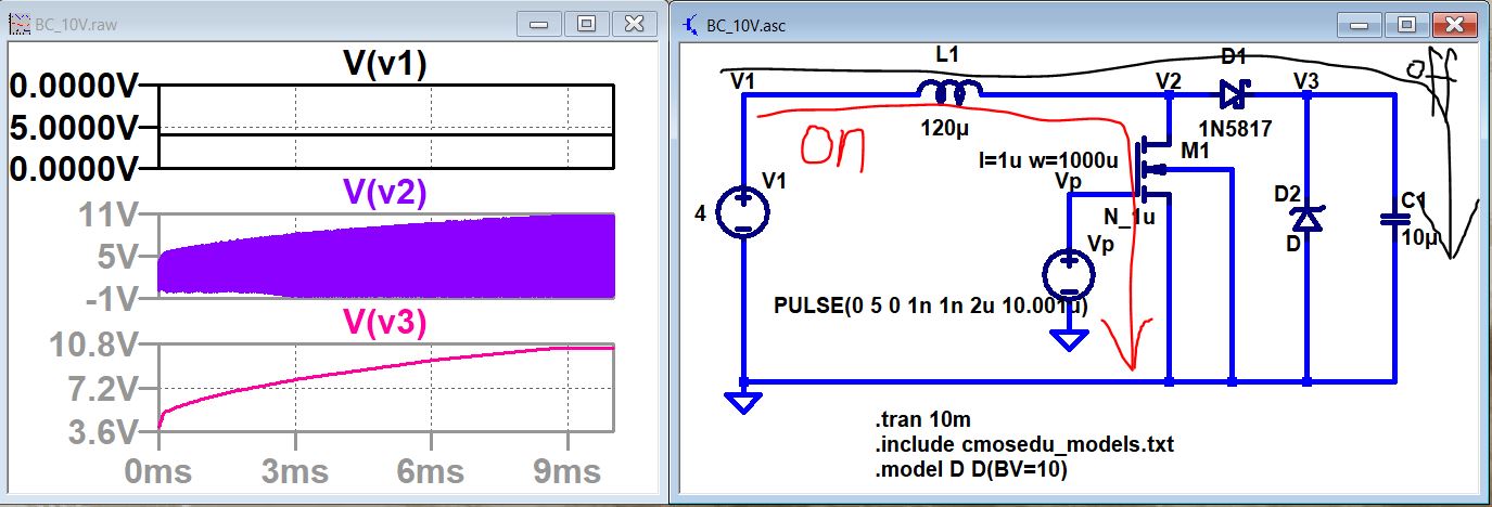
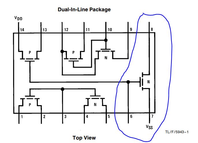
The datasheet for the transistor being used can be found here (CD4007):
ground VSS, power up the chip at VDD, and connect Pin 6 to the square
wave, connect Pin 8 to the same location of V2 in the simulation
schematic.

The
statement '.include cmosedu_models.txt' is a text file that defines the
fabrication parameters of the NMOS transistor (M1) we used in the
circuit. Here is the package you need for the simulation.
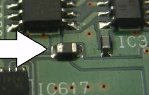
Keep in mind that the 'bar' painted on the diode indicates the cathode side of the diode.
Use
the electronic components available in the lab to build the circuit on
a bread board to test the input and output of the circuit. The purpose
is to boost a 4 V DC power to a 10 V DC powe supply using your
Boost Converter.
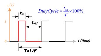
Make the input square wave to the transistor to be 20% duty cycle:
** Boost Converter Operations:
Step 1:
When the MOSFET is on, current goes through the MOSFET and then to the
GND. Energy is stored in the inductor in the form of a megnetic field.
The voltage polarity across the inductor is 'Left plus and Right minus.'
Step 2:
When the MOSFET is off, the previous megnetic field is destroyed and a
new one is generated: 'Left minus and Right Plus'. Then you'll get two
voltage sources in series so the output voltage is V1+Vind, this
voltage will charge up the loading cap. Because
the switch is turning on and off so fast, the inductors magnetic field
never fully collapses, so when the switch is opened again, this causes
a higher voltage on the inductor as it adds to the magnetic field.
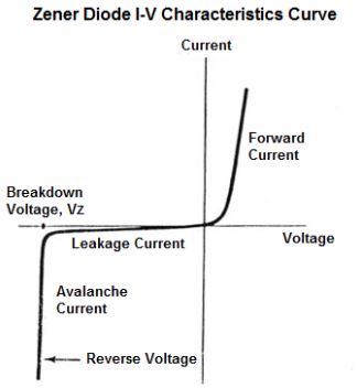
The statement '.model D D(BV=10)' defines the Breakdown
voltage of D2 (a zener diode). The function of the zener diode is to
stabilize the output at 10 V. See the diagram of the Zener diode: The one we are using today is 1N5240 ZENER DIODE. The regular diode we will use is 1N5817 S&P DIODE.
Don't
worry about these new things now, you just need to know there functions
in this circuit but not the details of their physics. These things will
be covered in ENGR 337 Analog Electronics.
*
For more advanced Boost Converters with a feedback and stable output
with a load, watch the video here
for your references. We do not have
time to build this in this lab. Also, if you have a passion to make a
product out of this and prototype it onto a PCB, try it yourself or
pursue this as your senior seminar project.
Follow the lab
report
guidelines
to avoid losing points.