Lab08 PSU Layout
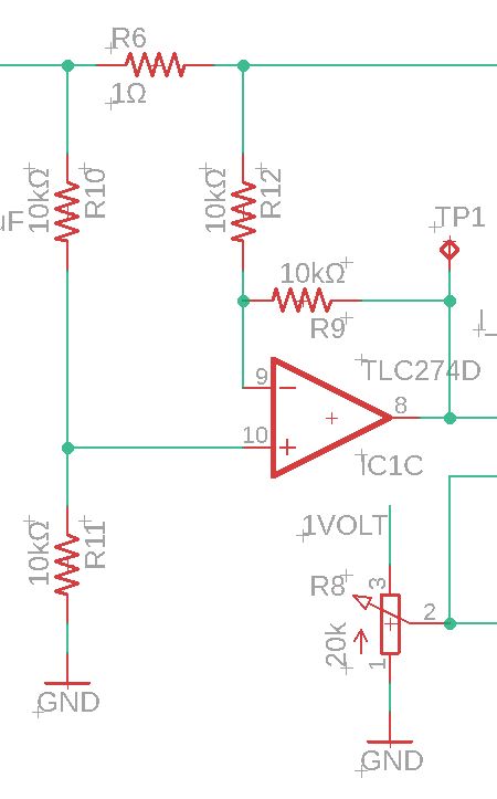
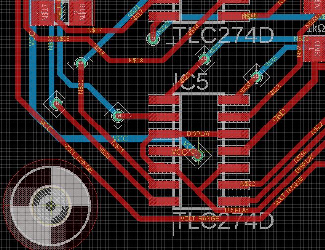
Circuit
layout for the difference (differential) amplifier is fairly critical, and it should be as symmetrical as possible
to ensure that stray capacitance affects both opamp circuits
equally. An asymmetrical layout may seriously compromise CMRR.
I
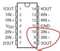
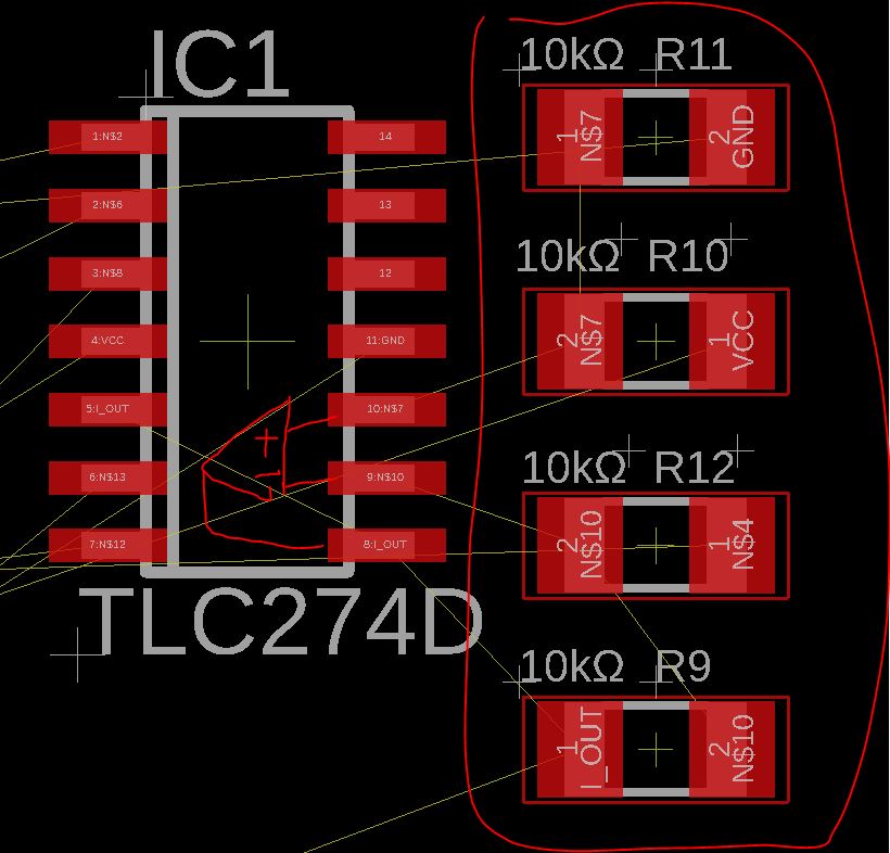
have the 3rd OpAmp in the chip used for the difference amplifier and it
is IC1C which is the one at the bottom right corner of the chip.
Setting the four resistors at the same distance from the two input pins of that OpAmp.
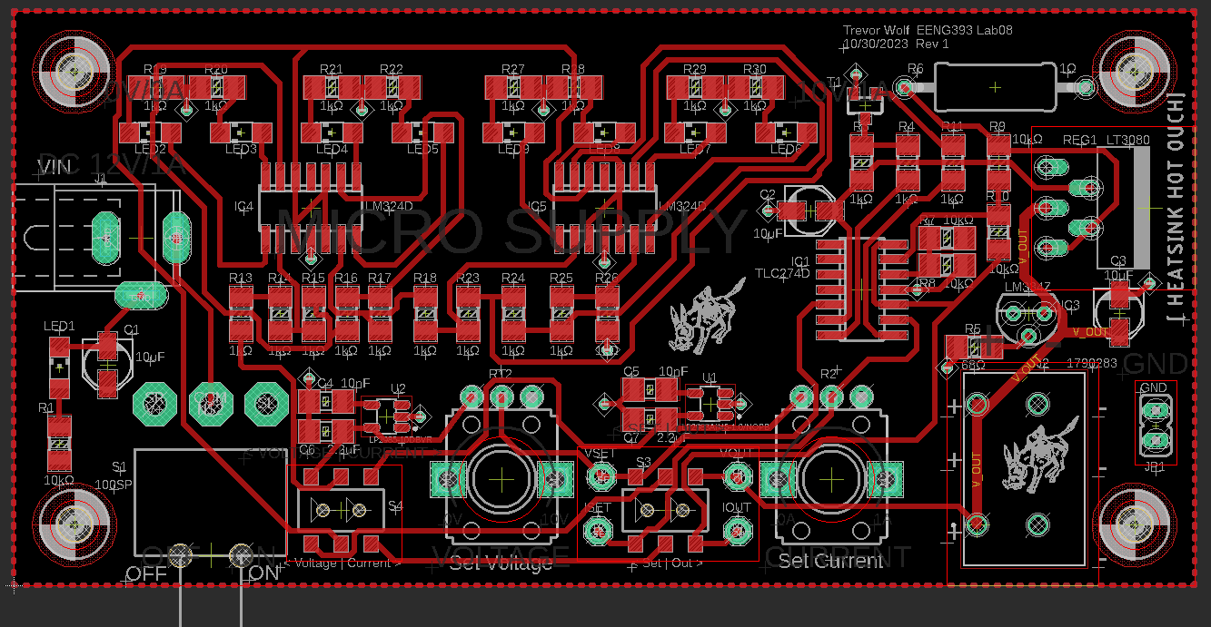
For
this simple PCB design, location of other parts is not that critical.
The one main principle is that keeping functional blocks within a
certain area, rotate the parts to keep the airwire less tangled, keep
power headers/connectors at the edge of the board, keep the drill holes
at the four corners, tall components shouldn't be too close to each
other (very hard to solder), resistors and capacitors serving a local
area should be aligned in a row, a column or an array depending on the
availability of the space on the board.
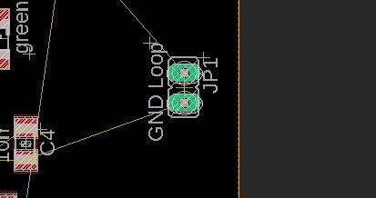
Move
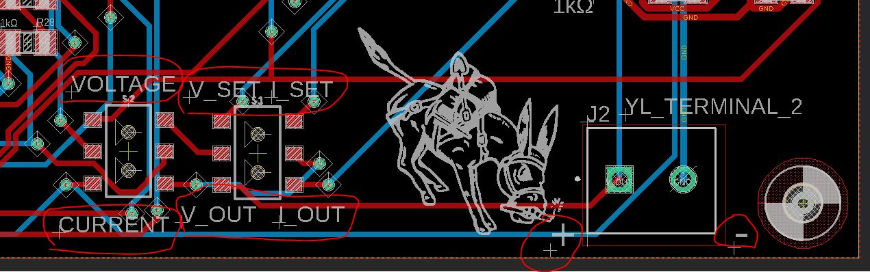
the four Tap pads to the edge of the board and keep them cloas to each
other. Also, add I_SET, V_SET, I_OUT, V_OUT in the 21 tPlace layer.

The GND loop should also be at the edge of the board.
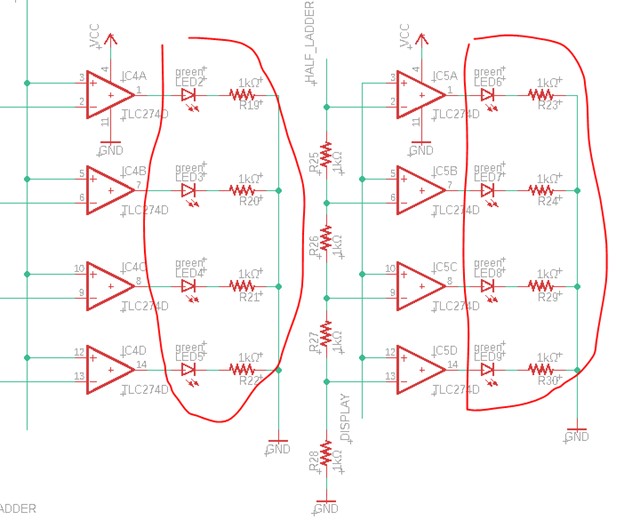
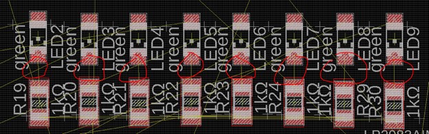
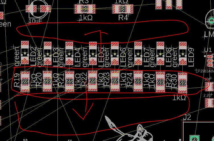
The following LEDs should be placed in a row or a column so
you can visualize the power change by looking at the LED ladder
The Layout as follows. Rotate them so they can make a direct
connection with a very short trace.
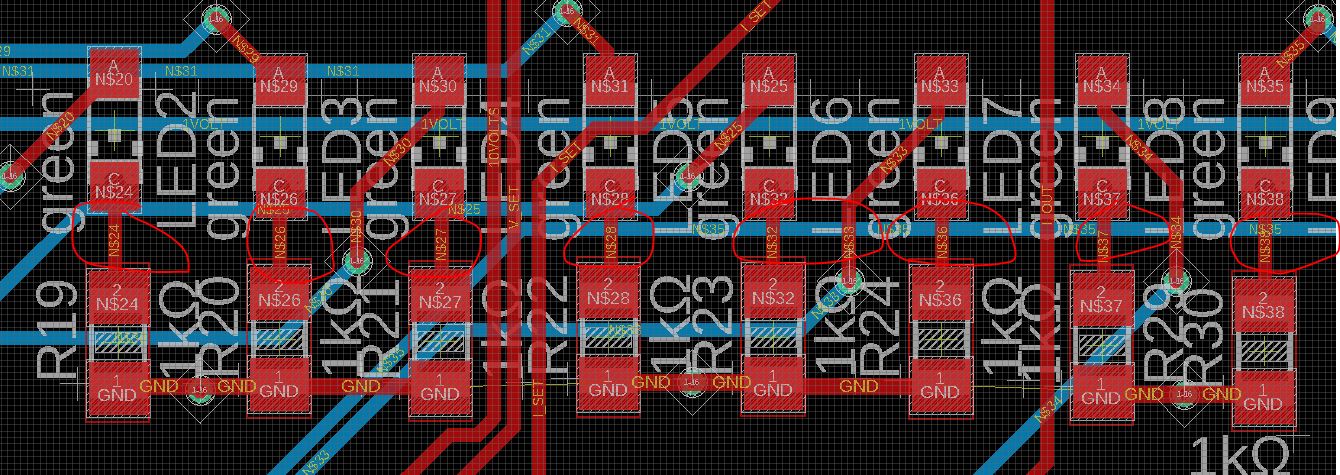
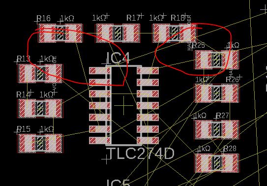
It resulted in the following connections in the middle. All direct connections without any lengthy traces and vias.
Have big empty space nearby? Yes, don't make your components to crowded, move them around.
Rotate
any parts that you think that will make the routing easier. Most of the
times you could easily tell from the airwire. You should avoid crossing
airwires as much as possible.

Avoid
creating dead corners like the ones shown below, as they will make
routing difficult. Simply disperse the components slightly to make the
router's job easier.
Bad:
The following one is a lot better than the one above.
Good:
Move
vias slightly away from the pad since they are bared metal and very
likely the solder you put on the pad will connect to these vias next to
them. Same for the wires, keep them a little away from them if
possible.
Here is the trad-off:
1. Thicks trace, lower voltage drop/loss
2. Thicker trace will take up more space and requie more vias
3. More vias incease the likelihood of short circuits or failed connections
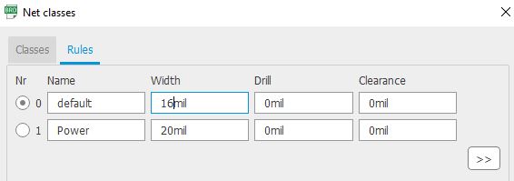
Set the VCC line and the GND line 16 mil which is slightly thicker than other regular traces.
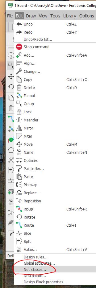
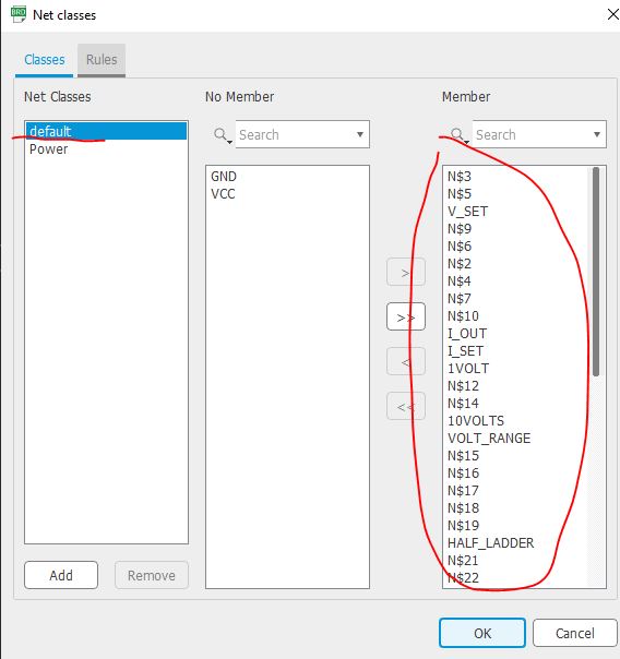
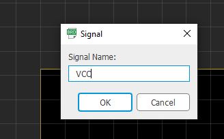
Add VCC and GND to the Power Class.
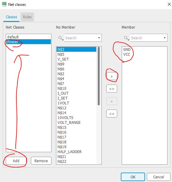
Also the default group includes all other nets.
Set the Default Class to be 16 mils thick and the power to be 20 mils thick.
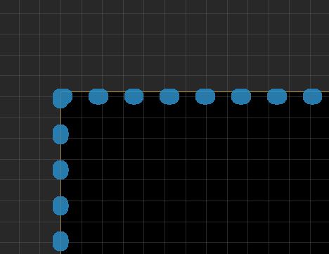
You
should avoid placing any vias too close to the pads, as shown in the
following layout. Well, what is the definition of 'too close'?
Let'schange the DRC rules.

You
can change the via clearance in your DRC rules. In this design, and
assuming that most of you are beginners at soldering surface mount
parts, please use at least 40 mils (about 1mm) as the clearance between vias and other components. When you are done, click Apply.
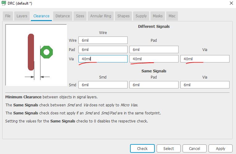
The
result should show similar clearance as follows. It's not that easy to
short the 1mm gap on a PCB unless you intentionally do so :-)
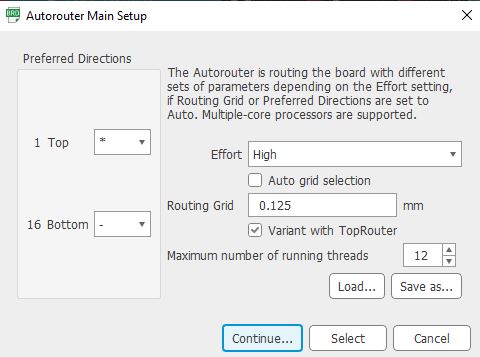
Please
note that manually routing it will create a much nicer layout than what
the auto-router can achieve. I didn’t have time to do it manually, but
I found a good example for you to follow. Let’s give a shoutout to TA Trevor Wolf for this!
For this design, I would just auto-route it and manually adjust it when needed.

Add the name/auther/version number of the board at the tPlace layer to the top of the board.

Two more things to adjust:
1.
Label the switch choices on the tPlace layer - when you choose either
current measurement or voltage measurement, you want to know where to
move the switch for that option.
2.
The Terminal header should be placed at the edge of the PCB. This
terminal is to supply voltage output so you want to make it easy to
access. The direction doesn't matter but label the + and - terminals
will be helpful for the user
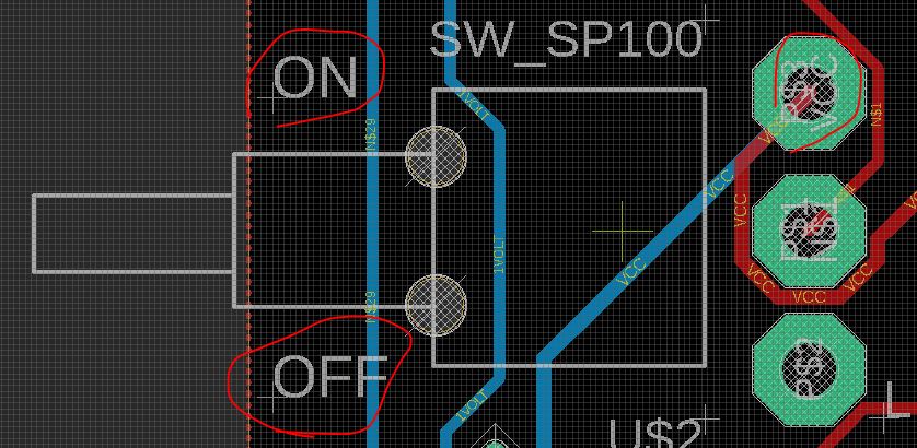
3. The SP100 also needs 'ON' and 'OFF" labels on the tPlace layer.
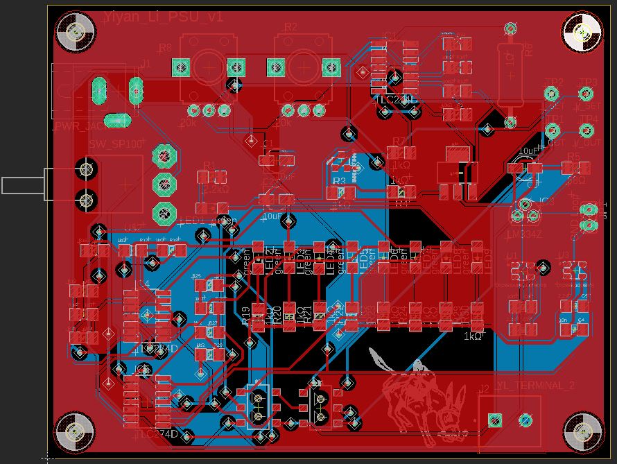
Compared to the snapshots above, I made further adjustments:
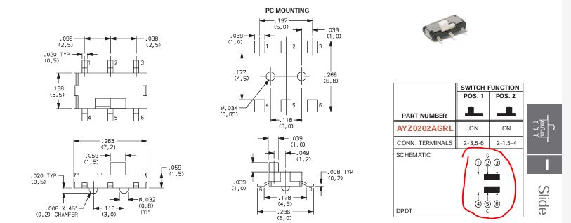
The DPDT switch footprint and internal connections.

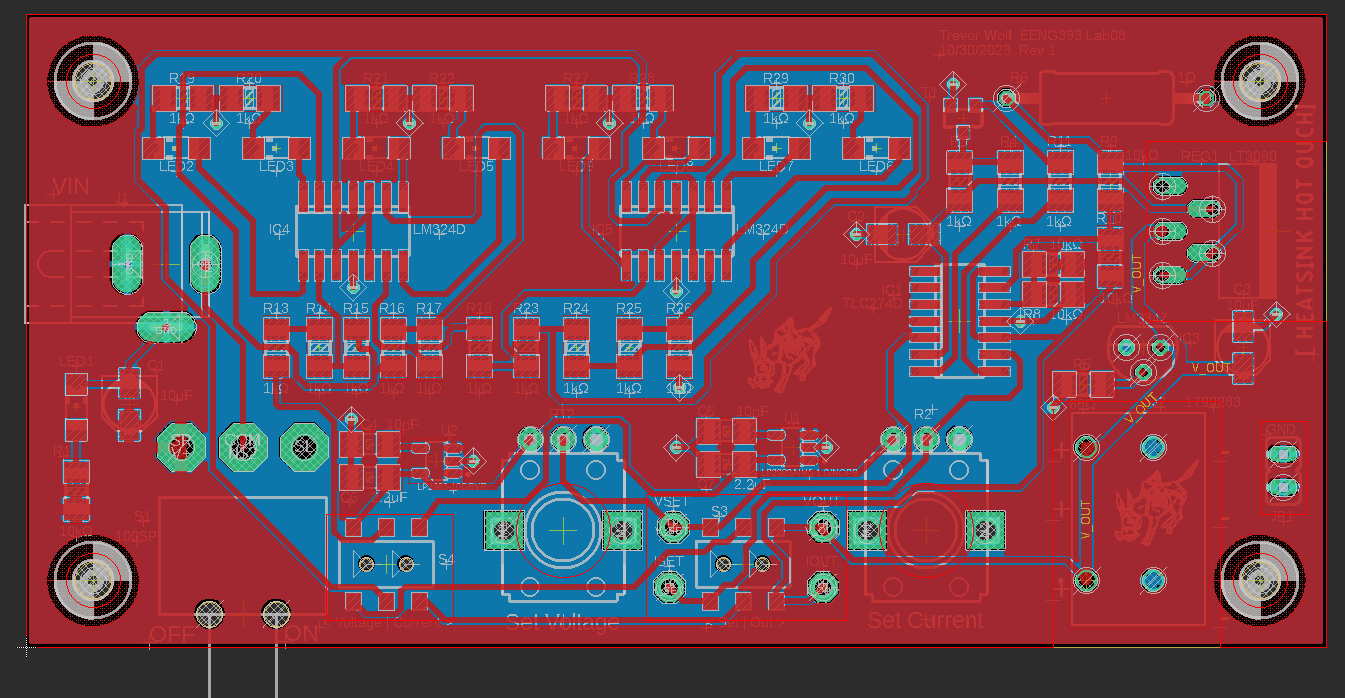
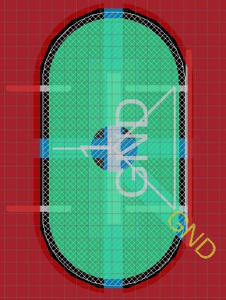
Place polygon at the Top and Bottom layers respectfully. Top polygon connected to VCC, bottom polygon connected to GND.
Note
that if you have to re-design your layout or re-adjust it, the correct
steps are: ripup all signals and polygons -> delete the polygons
(the outlines you drew) (not just ripup polygons but delete them) ->
adjust your layout -> re-route it -> re-draw the polygon outlines
to top and bottom -> ratsnest again -> DRC check.


Pour the copper.

Check if the VCC pads are connected to the top poured copper and if the GND pins are connected to the bottom poured copper.

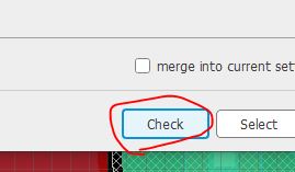
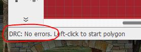
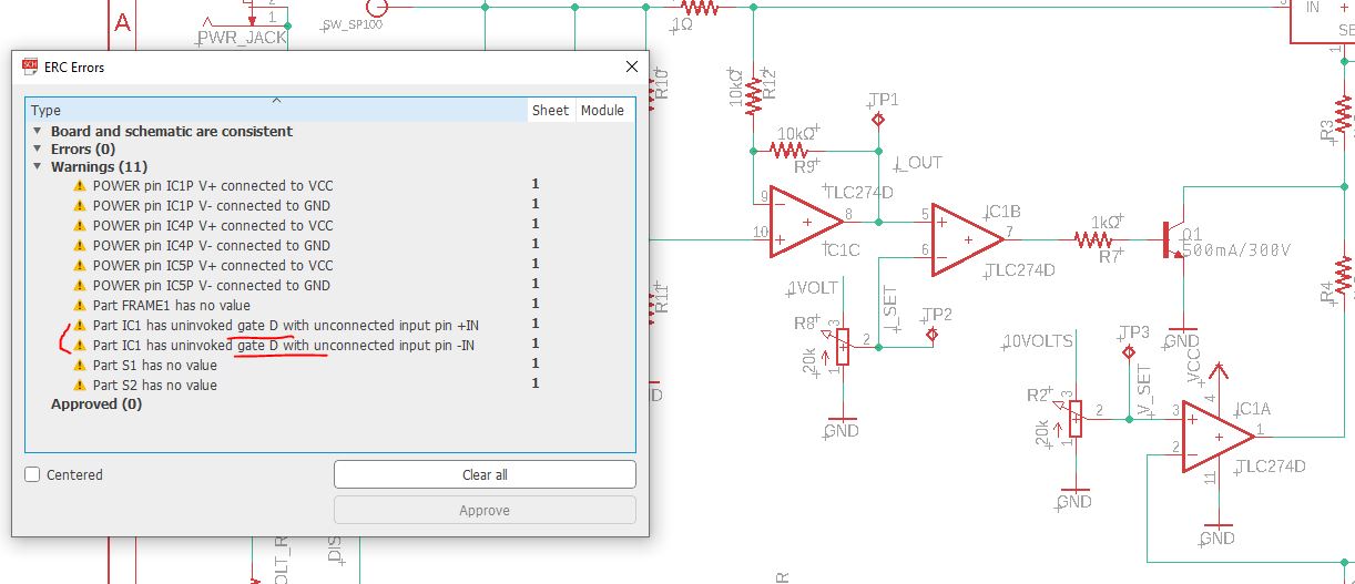
Run DRC and ERC.

No DRC errors.
ERC
warnings shown below are not any problems at all. The only one
attracted my attention a little is the IC1 D gates stuff. That is
because I didn't use IC1's D OpAmp at all.

Run the CAM processor to generate the Gerber files which are the PCB fabrication files define all the layers of the design.

For this simple project, I'll just use the default .cam template provided by Eagle.
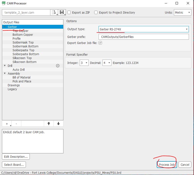
It'll generate a folder called 'CAMOutputs' to the designated directory.
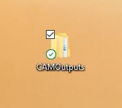
Place the drill file inside the DrillFiles folder to the GerberFiles folder.


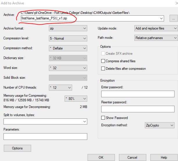
Get into the GerberFiles folder, select them all, right click and zip them into a folder.

Give it a meaningful name. For you project, you should name it as firstName_lastName_PSU_v1.zip.
Our
TAs will sit with you to review all the requirements on the rubric and
grade your layout. Only the checked and graded layouts will be
collected and sent out for fabrication. The deadline for submitting
your design to the TAs is Wednesday, 10/9, at 11:59 PM. If you can't
finish the design during the designated lab time, please reach out to
the TAs or visit during office hours to complete it.
My printed layout.
The following steps are for your future DIY projects. TAs and I will submit this project on your behalf.
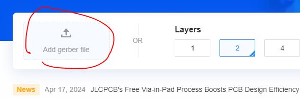
Submitting
to JLCPCB for fabrication is a very simple process. Simple add your
zipped gerber file to the portal, checkout using your credit card, and
it should take about 8 - 10 days for fabrication and shipping.
However,
in this class, the department will pay for your PCB fabrication so
please follow the instruction to submit your design.