Lab
2 Introduction
to FPGA.
Instructions:
(Please
note that you may not have Vivado in the following location if you use
the Lab desktop. Go to C:/Xilinx/Vivado/2017.3/bin/vivado.bat and
double click. It is being updated annually so use the newest version available on the C drive)
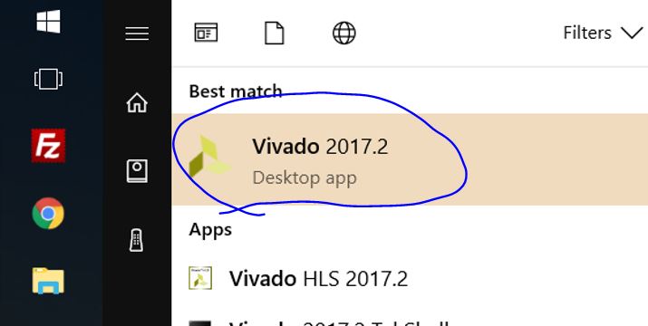
1. Open Vivado Webpack from your desktop (press the 'window' button on
the keyboard, and type 'vivado').
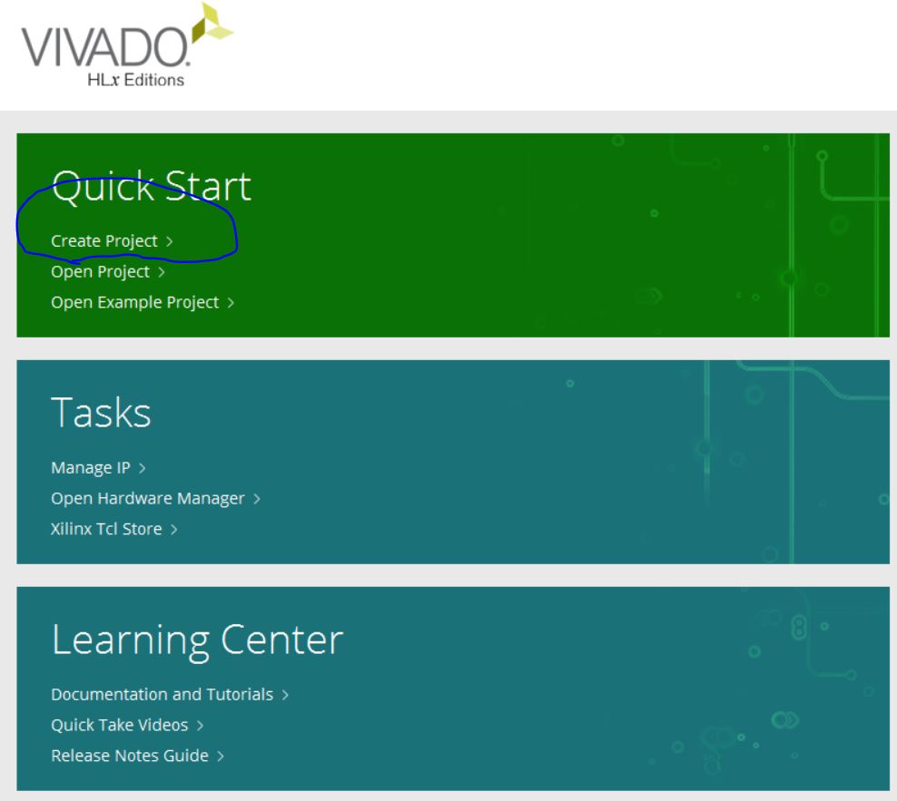
2. Create a new project:
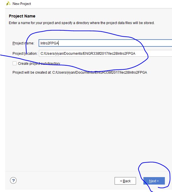
3. Put your project folder in a proper directory (no space in the
project name and the directory):
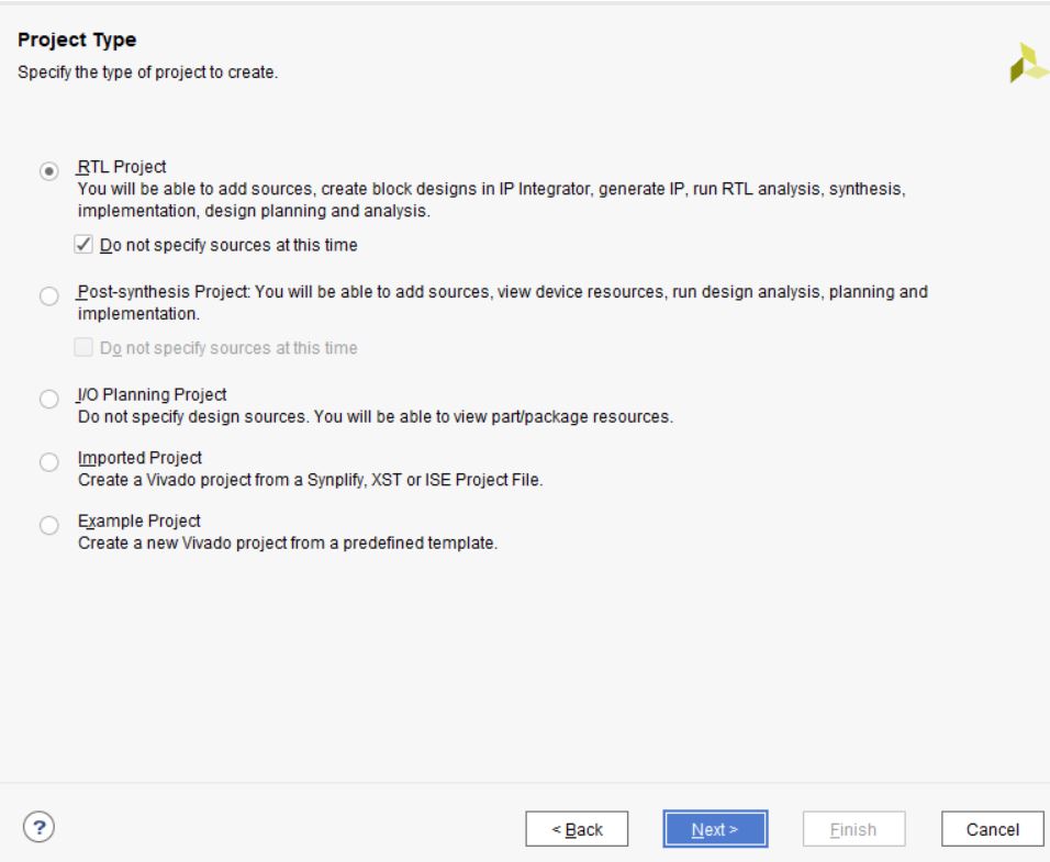
4. Select 'RTL' project:
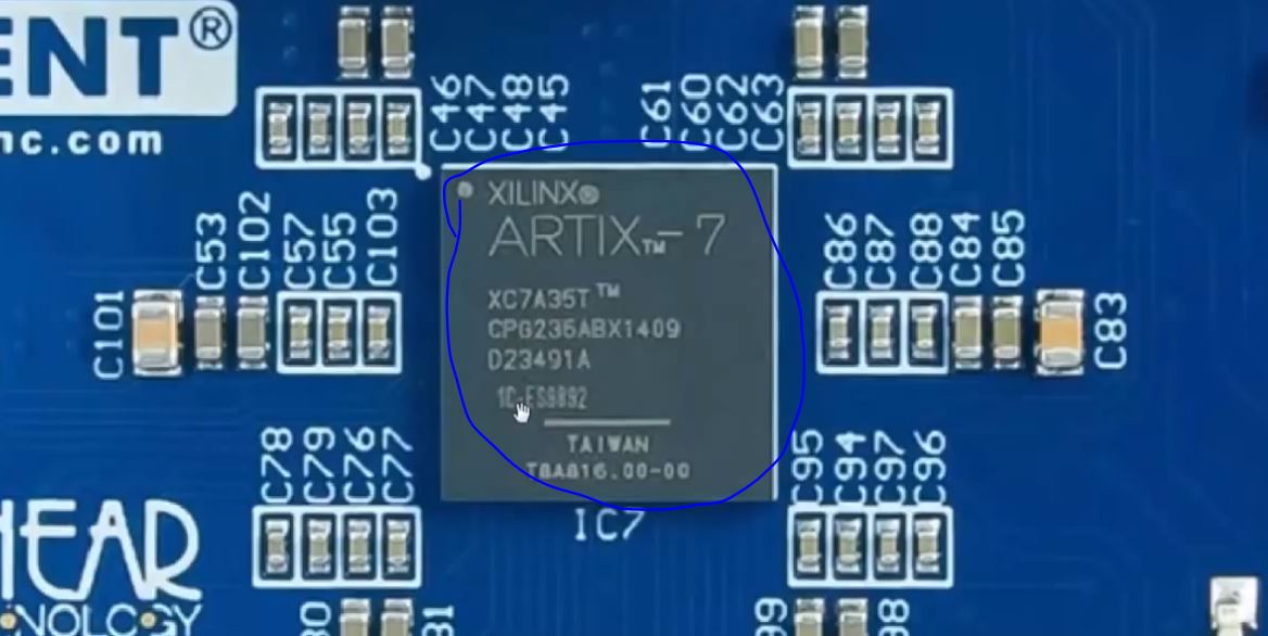
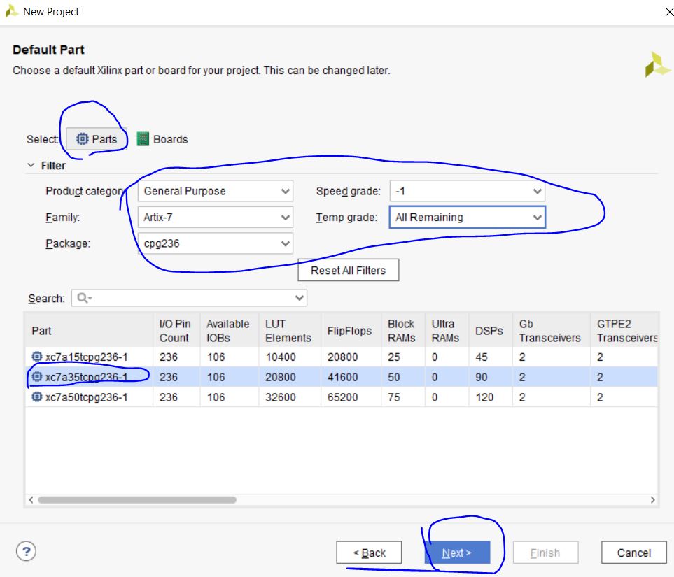
5. Select a proper chipset for your FPGA board. Our Basys 3 board has
an ARTIX-7 FPGA chipset, the part number is: xc7a35tcp236-1. Make
proper
settings as shown in the following figures:
Let's start making an AND gate using Vivado and FPGA!!
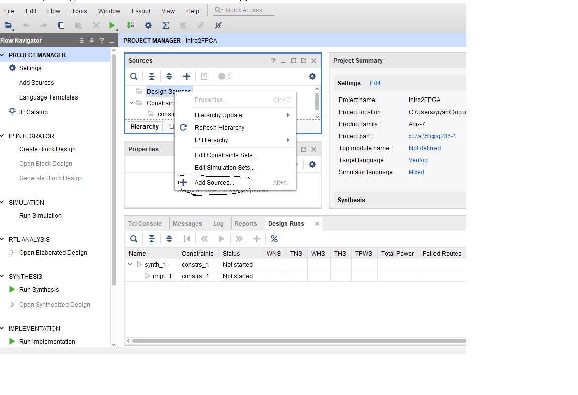
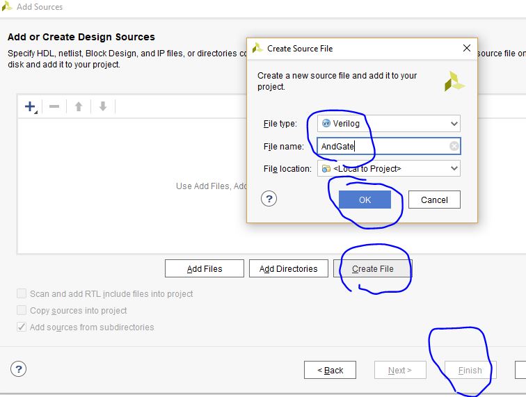
Right click 'Design Sources' in the Sources window, click 'Add
Sources'.
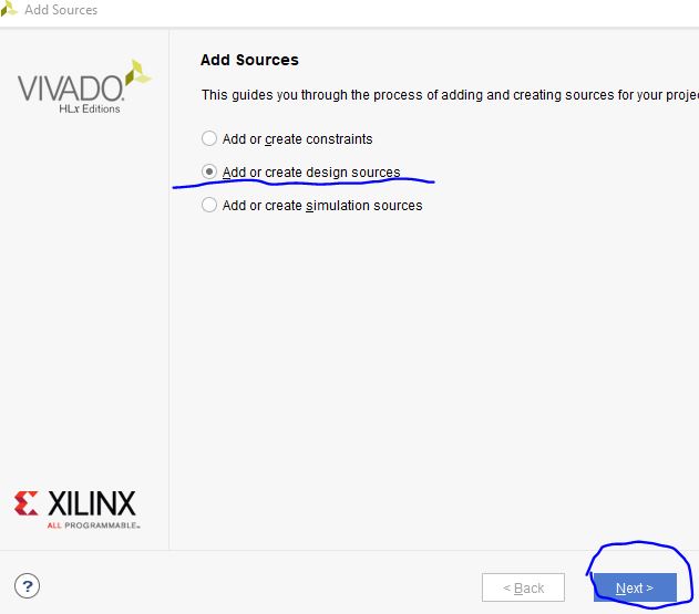
Select Add or Create design sources, and click 'Next'.
Create your first Verilog file, give it a name, and click 'Finish'.
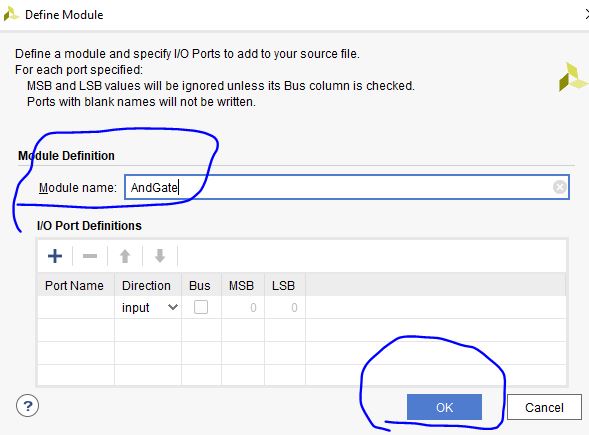
You've created a '.v' file in your project. Your
Vivado may ask you give a name to the module in the '.v' file. These
two names can be different. But in this example, there is no sense to
make them different, let's just call the module 'AndGate'. You don't
need to assign I/O port in this step, you can do it later. So leave
them blank, and click 'OK'.
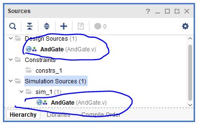
Now, the design file is created. You will see your files
in the
'PROJECT MANAGER'. There are three drop down menus, 'Design Sources',
'Contraints', and 'Simulation Sources'. For this 1st example, you
won't see anything in the 'Contraints' now. 'Constraints' defines the
pin map of the hardware. If we only do the simulation and see the
waveforms, we don't need it. But if we want to program the FPGA, we
need to define the pin map.
Double click 'AndGate.v' in the 'Design Sources' dropdown menu,
you will see the code editor window on the right.
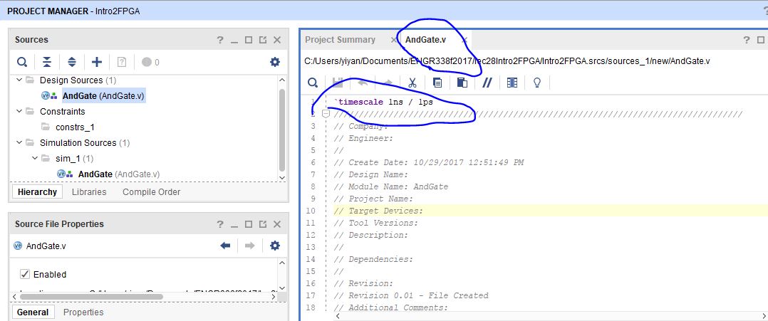
Now, you can type your verilog code in the window:
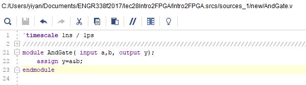
`timescale
1ns/1ps means that all the delays that follow (like# 5.1234) are
interpreted to be in nanoseconds and any fractions will be rounded to
the nearest picosecond (5123ps).
The next step is to verify the logic using simulations. We need a
testbench (a top module) to pack up this 'And Gate'. Just imagine this
module is a real logic gate you used in the lab, they have 2 inputs and
1 output, but no sources and signals. The gate should be conneted to
outside sources to verify the logic.
Now, let's add a testbench for this AndGate. It is the same way as you
add a regular '.v' source, but let's name it as 'testbench_andgate' to
distinguish it from other design files.
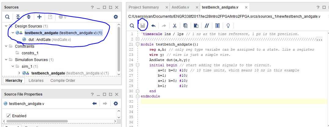
Now you have your testbench added in the source file. But Vivado won't
be able to know this testbench is for your AndGate. After we coded it,
Vivado will automatically detect the hierarchy for these two files, and
make the testbench as the top level layer, and the design file as the
'Device Under Test (DUT)'.
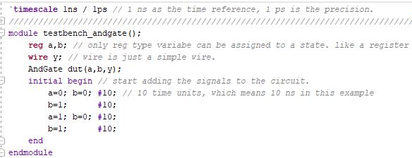
'wire'
elements must be continuously driven by something, and cannot store a
value. Henceforth, they are assigned values using continuous assignment
statements. 'reg' can be used
to create registers in procedural blocks. Thus, it can store some
value. 'reg' elements can be
used as output within an actual module declaration. But, 'reg' elements cannot be connected
to the output port of a module instantiation.
Afer the coding is done, click the 'save' button, the hierarchy will be
updated automatically:
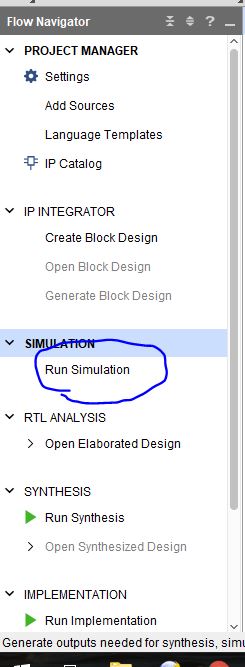
Now, it is ready to simulate the testbench and the DUT.
Click Run Simulation in the 'Flow Navigator'. It will run for several
seconds, then a waveform window will show up. You need to move the
scrollbar to the left to look at your logic. If it is still not
visible, press 'contrl + scroll the mousewheel' to zoom-in or zoom-out
the waveform view.
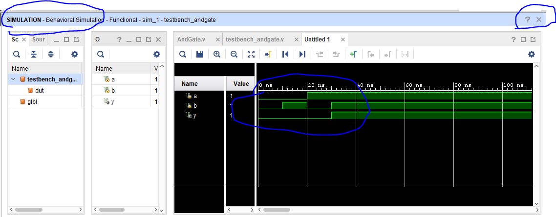
If
the logic is correct, fee free to turn off the simulation window.
You'll find the window above is 'SIMULATION', not 'PROJECT MANAGER' any
more, so feel free to close it then it will bring you back to 'PROJECT
MANAGER'.
Congratulations, you have completed the first simulation using Verilog
in Vivado. A good start.
Next, let's program your FPGA.
To
make a testbench in FPGA instead of a 'virtual simulation' in Vivado,
we will need a different testbench, and of course, we'll need the
constraint files to define the pins in FPGA.
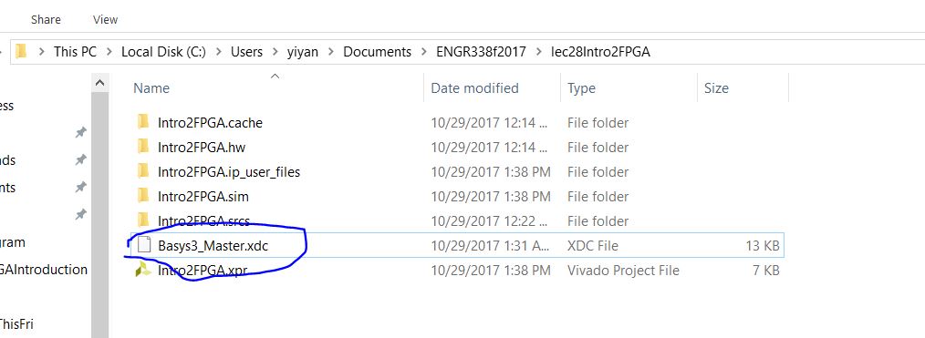
Add the contraint file:
Download the constraint file here
The
file name is Basys3_Master.xdc, put it in your project directory. You
can also copy the code, and paste it in a .txt file, and change the
extension to .xdc.
Right
click the 'Constraints' dropdown menu, click 'Add Sources'. In the next
window (not shown) click 'Add Files'.
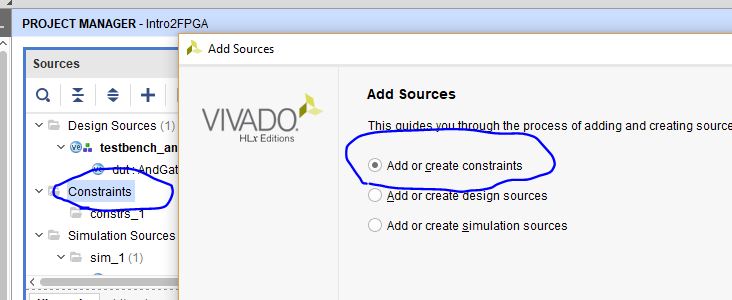
Find
out the constraint file and add it to the menu. (if it is not showing
up, check the bottom if you have selected 'All Files' for the 'Files of
type' at the bottom):
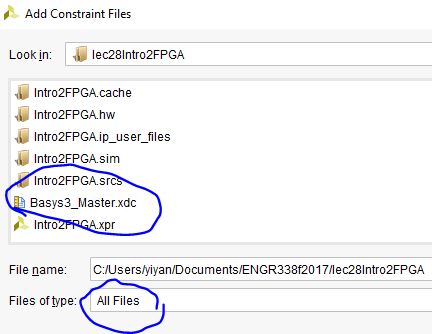
Add the constraints and click 'Finish' at the bottom.
Double click the constraint file in the menu, you will see the code in
the editor:
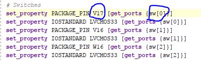
'V17'
is the real pin number of the FPGA, sw[0] is the LSB of the 16-bit
swithces on the board. This means the hardware pin 'V17' is already
connected to sw[0]. The same concept applies to the LEDs and other
pins.
Of course, you can comment all the constraints that you
won't use for your project. For this example, if we want to connect the
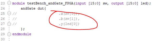
inputs of our And Gate to b=sw[1], a=sw[0], output y=LED[0],
then
we can use the swithces on the board to provide logic 0 and 1s, and
look at the LED to verify the logic. So we can comment all other
constraints except for sw[15:0] and LED[15:0]. (keep other sws on even
you won't use them, they should be an entire group to be declared in
your verilog code).
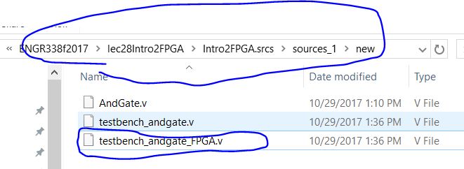
Go to your .srcs directory in your
project directory, and add a new '.v' file. I suggest copy and paste
your testbench_andgate.v file, and rename it as
'testbench_andgate_FPGA.v'.
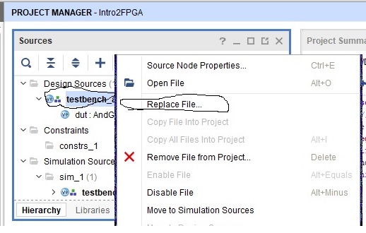
Then go to Vivado, right click your old testbench, and select 'Replace
file'. Then find your new testbench file to replace the old one. The
new testbench is used for the real hardware but not simulation.
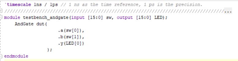
Now, let's change the code in the new testbench. Remember double click
the new testbench to open it in the editor, otherwise you will be
editing your old testbench.
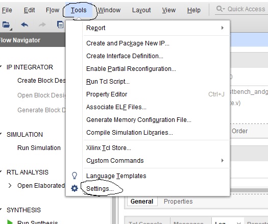
Go to Tools-Settings
Check the box in Bitstream - -bin_file.
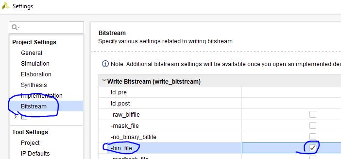
The
purpose of this step is to generate both the .bit file and .bin file
for programming. We will use them in the following experiments.
Run Synthesis by clicking 'Run Synthesis' on the left
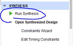
This will take a couple of seconds to run. If a window pops up then
check 'Run Implementation'.
The
Vivado Design Suite implementation process transforms a logical netlist
and constraints into a placed and routed design, ready for bitstream
generation. The implementation process consists of the following
sub-processes.
When it is done, a window
will pop up. Check 'Open Implementation'.
Then go to Tools - Edit Device Properties
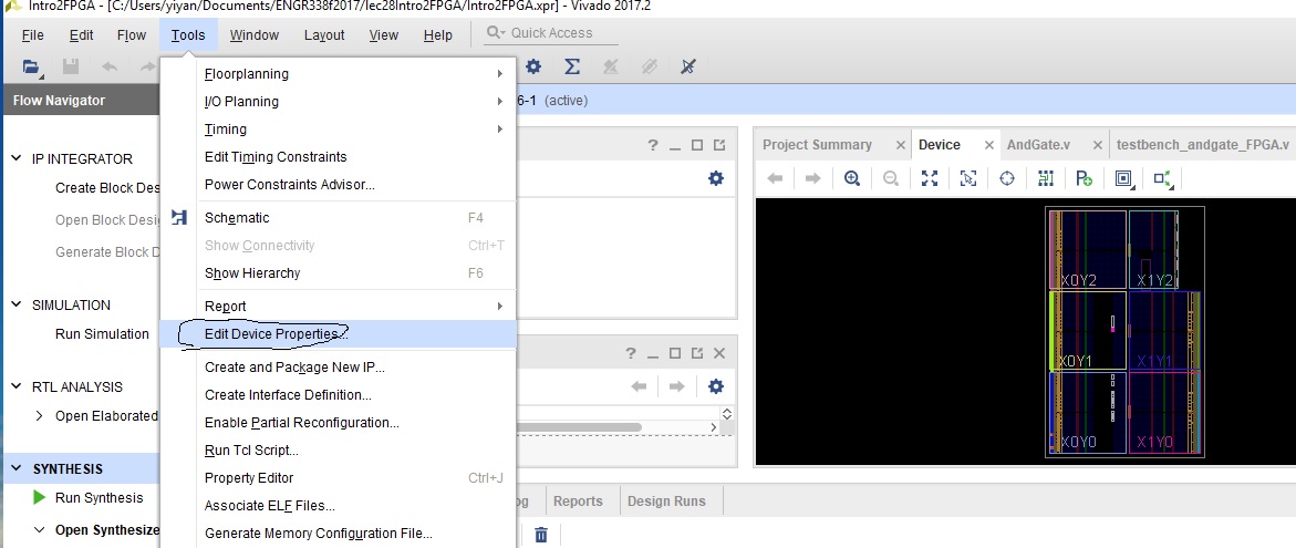
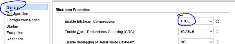
General - Enable Bitstream Compression - True
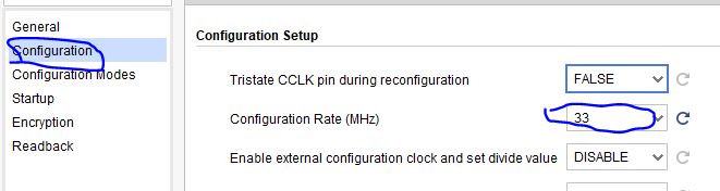
Configuration - Configuration Rate (MHz) - 33 MHz
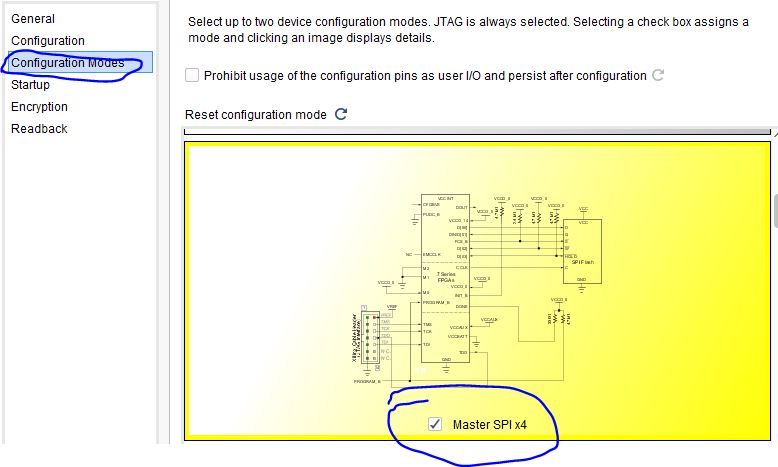
Configuration modes - Master SPI x 4
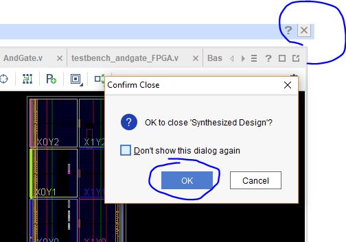
Close the 'SYNTHESIZED DESIGN' window, and save the chnages
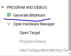
Generate Bitstream
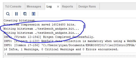
Make
sure there are not errors, and both the .bit file and .bin file are
generated successfully. .bit file is used to program the FPGA from your
JTAG wire. If you power off your FPGA, all the program will be gone.
However, .bin file can be saved on an on-board memory, which can be
saved permanently until you flush if with another .bin file.
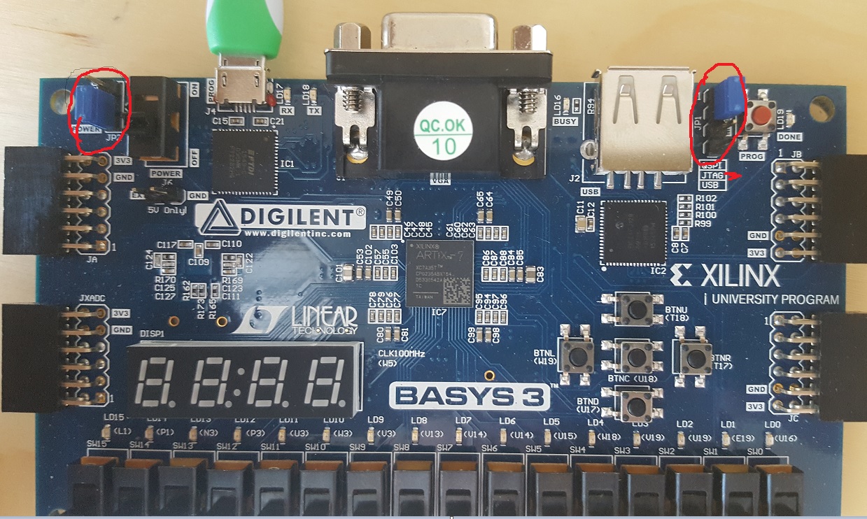
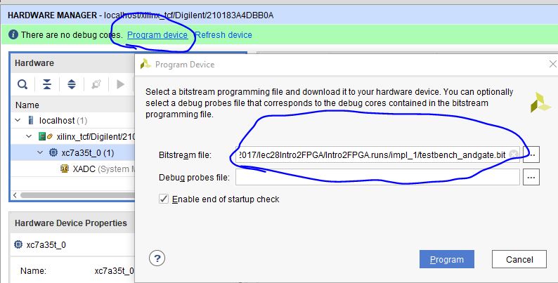
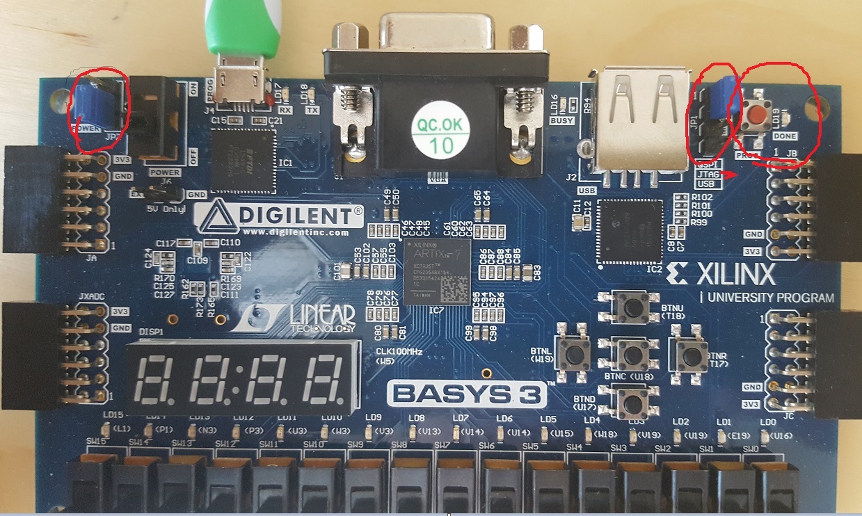
Open Hardware Manager, make sure your FPGA is connected to your
computer using a microUSB cable. Also, put the jump wire on the JTAG
spot (the jump wire position in the figure below is not correct for
programming from the computer, you need to move it one step down).
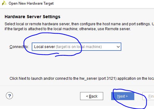
Go the navigation menu on the left, Open Hardware Manager:
Program the device
Now,
a tiny 'And Gate' is synthesized on your FPGA chip. Imagine how cool it
is. You will never need to use the bulky ICs to wire everything on the
breadboard. This single tiny chips can implement huge logic for you!
Try your sw[0] and sw[1] on the board as the inputs for the And Gate,
to control teh LED [0].
Before
we wrap up this lab, let's try to use the on-board memory to program
the chip instead of using your computer. If you power off your board,
the program will be gone. But the .bin file in the on-board memory can
be stored permanently.
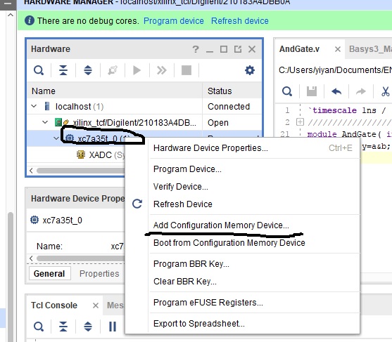
Pragram the chip using the on-board memory.
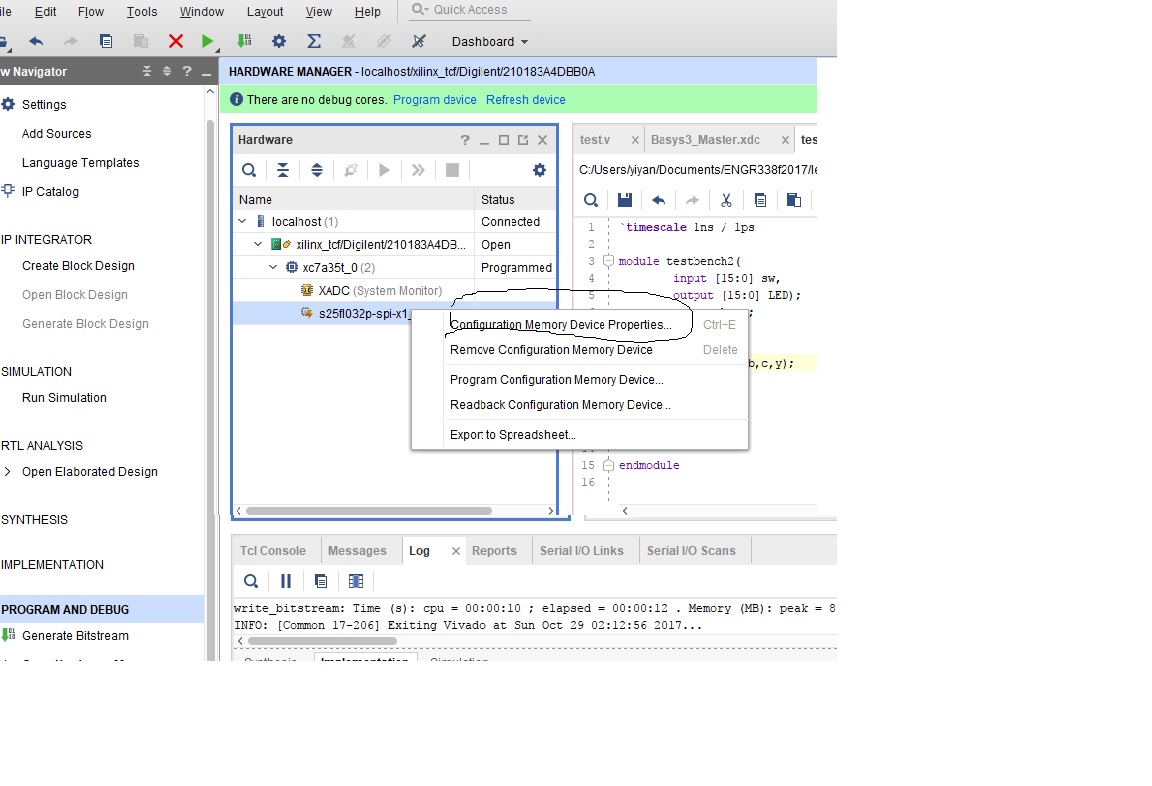
Right click your device in the Hardware window and select Add
Configuration Memory Device....
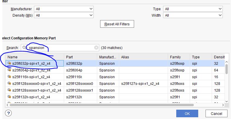
In the next window, type 'spansion' in the search engine, and select
the one that has 32 bits for the density
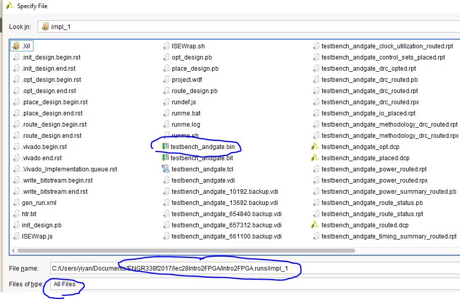
In the next window, select the .bin file you generated just now:
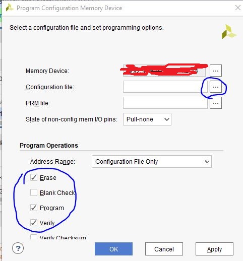
Then,
the on-board memory just received all your program .bin data. Now,
let's change the jump wire to QSPI, and push the push button 'PROG'
beside the jump wire on the board.
Now, you won't lose your logic if you power off the board.
Other things you need to know before you leave:
1. When program the board using .bin file from the on-board memory, the
Jump Wire has to be set at the QSPI spot. Otherwise, nothing can be
programmed and the previous data will be flushed.
2. When program using the .bit file, the Jump Wire has to be at the
JTAG spot.
3. If the .bin file is updated, right click the memory device and
configure the file again
Congratulations,
this simple 'And Gate' example for both Simulation and on-board
verification is done. You will be ready for a larger project using FPGA
in the future.
----------------------------------
Tasks:
1. Go through all the steps in this lab instruction, report your code,
simulation results, and the on-board verification results. (30 points)
2. Use the same procedure to create XOR and OR gates. Run simulations to verify the logic. (30 points)
3. Use both the volatile and nonvolatile methods (QSPI) to program your FPGA. Show videos for the demonstrations. (40 points)
** A summary on the different
programming techiniques on the BASYS 3 board:
1. Jump wire to JTAG is to program the FPGA chip and the on-board
memory. So you need to do this first.
2. Keep the Jump Wire at JTAG, unplug the USB cable to power it off.
Then power it up again, the logic should disappear.
3.
Chage the Jump Wire from JTAG to QSPI, then press the Red Push Button
on the right 'PROG'. This will program the FPGA again and this won't
disappear after you power it off and back on.
4. Keep the same code structure, delete the marked part as follows:
Then
repeat the process above to re-generate the bit file and the bin file
and program the memory using this invalid code to clean out the memory.