Lab
7 The Universal Serial Bus (USB) Interface on Basys 3
1.
Basics
The
user presses a key on the keyboard, this sends a keyboard PS/2 scan
code to the Basys3 over the USB-HID port. This scan code is read and
transmitted to a terminal application via the USB-UART bridge. When the
key is released, a scan code of F0XX is transmitted, indicating that
the key with PS/2 code XX has been released.
The Basys 3 board
has a PIC24FJ128 microcontroller that provides USB HID host capability.
We will use this option to develop the HDL projects here. Specifically,
we will focus on interfacing a keyboard to Basys3 board since the
PIC24FJ128 chip available on the board converts the USB input to
standard PS/2 signals to communicate with a mouse or keyboard. Here,
the Basys3 board will be the receiver. The keyboard will be the
transmitter. Therefore, we will focus only on the USB-receiving module
next.
The transmitted
code is
called a scan code and is further sub-classed as a 'make' code in the
case of a key being pressed. If a key is held down without being
released, the make code for that key will be sent continuously, in
accordance with the defined auto-repeat (typematic) rate. It should be
noted that if more than one key is pressed and held down, typematic
mode only applies to the last key pressed. When a pressed key is
released, an additional scan code is sent to the host to let it know
that the key that was pressed has now been released. This additional
transmitted code is called a 'break' code.
The
Microchip PIC24FJ128 microcontroller on the Basys 3 board serves as an
auxiliary controller, primarily responsible for USB HID (Human
Interface Device) host capabilities and FPGA configuration. It handles
the USB protocol for connected mice and keyboards, translating HID data
into a standard PS/2 interface for the FPGA. Additionally, it manages
the process of loading FPGA bitstreams from a USB drive connected to
the J2 port.
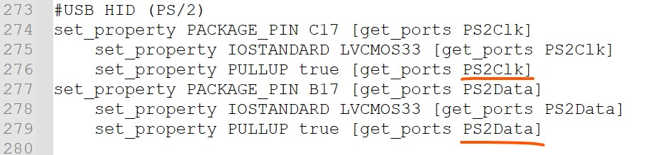
The constraint file shows the two pins relevant to the HID
In the following two windows, the right one is an USB receiver, the left one is a top module.
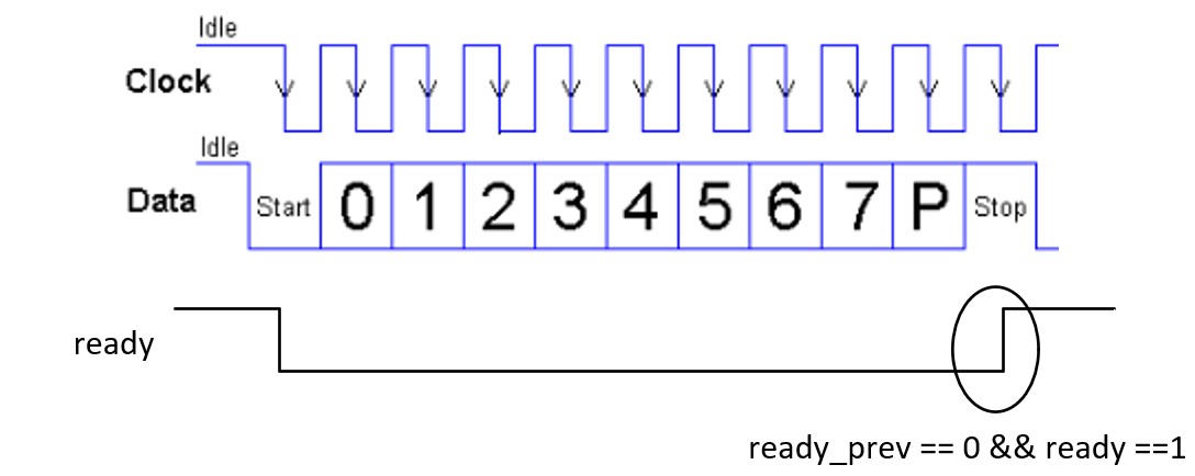
It's very helpful to know the timing diagram of the ps2data and the ps2clk:
Receiving
of each bit is synchronized to the falling edge of the clock. Our
submodule (on the right hand side) does have 'negedge' on the
sensitivity list. According
to the code in top module (USB_keyboard_app), only when ready_prev == 0
&& ready ==1 the data is being taken in. That makes perfect
sense on the timing diagram. This is exactly the moment that the data
and the parity bit transmission are completed.
The
keycode in the make code is not used at all so why it still stores the
keycode in both the make code area and the break code area? Keycodes
are sent twice—once for the "key down" event and once for the "key up"
event—to allow software to distinguish between a momentary tap and a
sustained hold. The operating system monitors the time difference
between these events to determine if a user is typing a single
character or performing a "long press" to trigger auto-repeat
functionality. There isn't an operating system on the FPGA chip so the
make code during bits [23:16] is not used.
In the "STOP"
state, the
partiy checker is an odd parity checker. Line 39 means it reports error
if bit "prty" is not equal to ~^received.
The
demonstration:
2.
Send the Scan Code to a seriial terminal
We can combine
the UART tx module here to display the key values on the serial
monitor.
Draw the system
diagram helps the desgin of the RTL:
Here is the
video demonstration.
--------------- Tasks: 1. Repeat the
work in Section 1. (10 points) 2. Design the
testbench and the scan code to ASCII converter to display key values on
the serial monitor. (90 points)