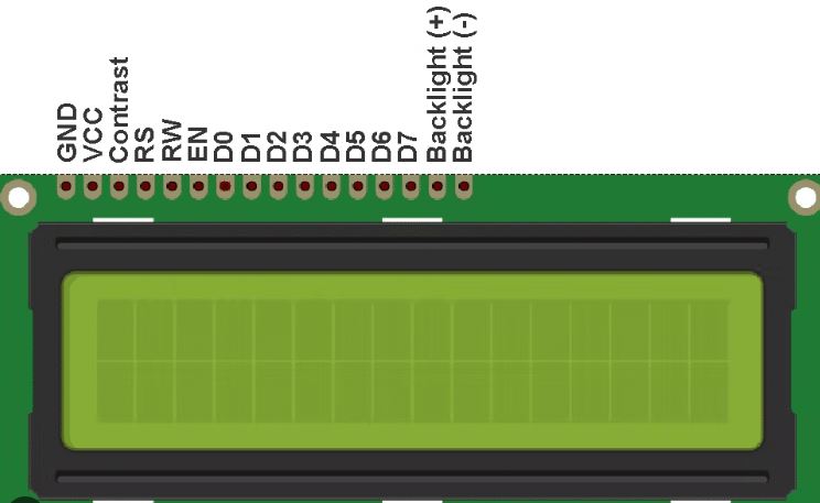
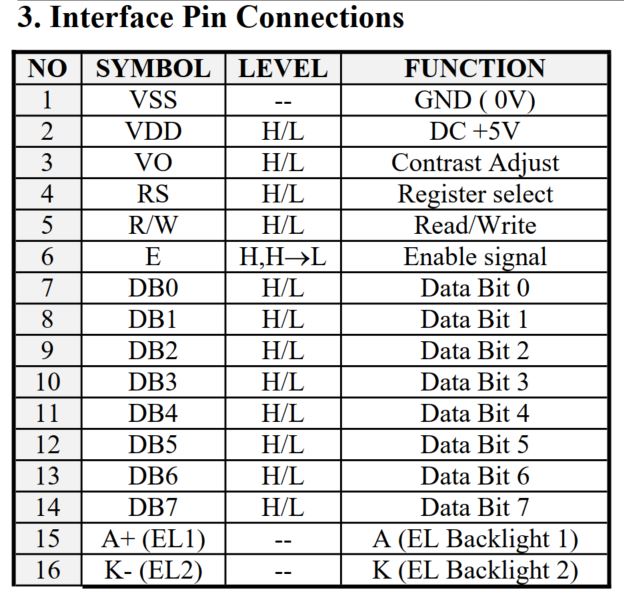
The
GND (VSS) and VCC (VDD, +5 V) pins are the power supply pins. The VO
pin is used to adjust the display contrast. We can use a potentiometer
to connect VO to a suitable positive voltage below +5 V. The Led+ (A+)
and Led- (A-) pins are used to turn on the display backlight (connect
them to +5 V and ground, respectively).
The
RS pin is the Register Selector pin for the LCD controller. The HD44780
has two registers: an Instruction Register (IR) and a Data Register
(DR). The RS pin is a control pin that specifies whether the IR or DR
should be connected to the Data Bus (DB0 to DB7 pins). When RS is low,
the IR is selected and DB7-DB0 are treated as an instruction code. For
example, the instruction code can represent a “display clear” command.
When the RS is high, the DR is selected and DB7-DB0 are treated as
data. In this case, DB7-DB0 can be the code for representing a
character such as “a”.
The R/W pin specifies whether we are writing to the module (R/W=0) or reading from it (R/W=1).
The E pin (for “Enable”) starts a read/write operation.
The
following timing diagram may look complicated but they are actually
very simple. For the Write Operation, having RS ready first, then
The
timing diagram shows that we should set the RS and R/W pins to
appropriate values and wait for tAS( which should be greater than 40
ns) before setting the E pin to logic high. According to the table, the
E signal should have a width (PWEH) greater than 230 ns.
Then,
the E signal should have a high-to-low edge which starts a write
operation. Note that tDSW before this edge the data must be valid.
Besides, after the falling edge of E, the control signals and the data
should not change for some time denoted by tAH and tH in the figure.
Another important issue is the “Enable Cycle Time” which should be
greater than 500 ns. This shows that we should wait for some time
before starting to do the next read or write operation.
The LCD_driver.v
example provided by the textbook uses 1 ms delay before the 'en' pin to
be pulled down to ground which is an overkill (only requires about 550
ns). However, it is a good example for this lab.
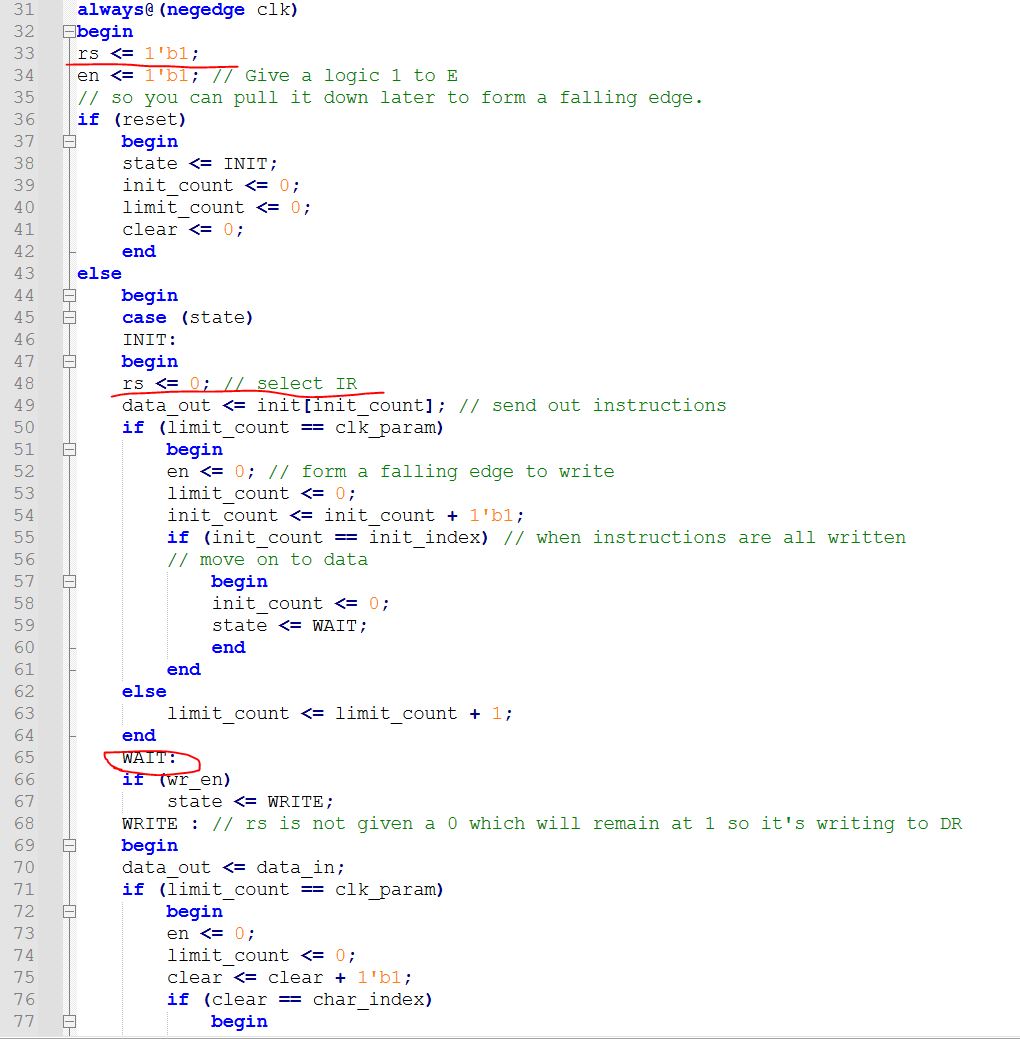
'rs'
is set at '1' every time posedge of clk arrives. In the INIT state, rs
is pulled down to ground so it writes data_out to IR; In the WRITE
state, rs is not pulled down to ground which means the rs==1 will
remain unchanged so it writes to DR.
Task 1: Repeat the work on the textbook (40 points)
Task 2: Modify the code to show steady texts on the display (30 points)
Task 3: Use ASCII code instead of letters in the code to display 'Hello !!'. (30 points)