Lab
2Program an FPGA, on-board memory,
and running LEDs
Next, let's
program your FPGA.
To
make a testbench in FPGA instead of a 'virtual simulation' in Vivado,
we will need a different testbench, and of course, we'll need the
constraint files to define the pins in FPGA.
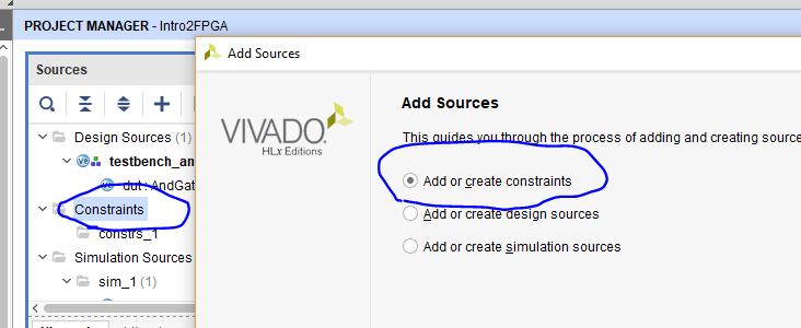
Add
the contraint file:
Download the constraint file here
The
file name is Basys3_Master.xdc, put it in your project directory. You
can also copy the code, and paste it in a .txt file, and change the
extension to .xdc.
Right
click the 'Constraints' dropdown menu, click 'Add Sources'. In the next
window (not shown) click 'Add Files'.
Find
out the constraint file and add it to the menu. (if it is not showing
up, check the bottom if you have selected 'All Files' for the 'Files of
type' at the bottom):
Add the constraints and click 'Finish' at the bottom.
Double click the constraint file in the menu, you will see the code in
the editor:
'V17'
is the real pin number of the FPGA, sw[0] is the LSB of the 16-bit
swithces on the board. This means the hardware pin 'V17' is already
connected to sw[0]. The same concept applies to the LEDs and other
pins.
Of course, you can comment all the constraints that you
won't use for your project. For this example, if we want to connect the
inputs of our And Gate to b=sw[1], a=sw[0], output y=LED[0],
then
we can use the swithces on the board to provide logic 0 and 1s, and
look at the LED to verify the logic. So we can comment all other
constraints except for sw[15:0] and LED[15:0]. (keep other sws on even
you won't use them, they should be an entire group to be declared in
your verilog code).
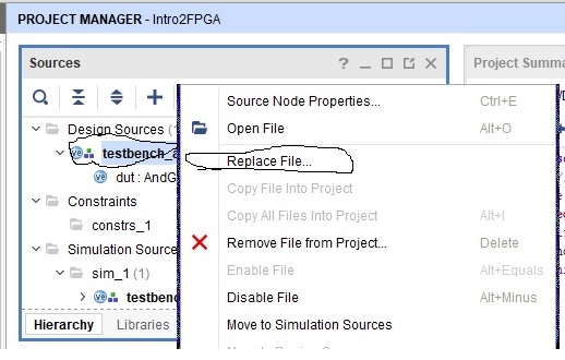
Go to your .srcs directory in your
project directory, and add a new '.v' file. I suggest copy and paste
your testbench_andgate.v file, and rename it as
'testbench_andgate_FPGA.v'.
Then go to Vivado, right click your old testbench, and select 'Replace
file'. Then find your new testbench file to replace the old one. The
new testbench is used for the real hardware but not simulation.
Now, let's change the code in the new testbench. Remember double click
the new testbench to open it in the editor, otherwise you will be
editing your old testbench. Please note
that the
constraint file from this website uses "LED" but the constraint file
from the lecture's website uses "led". I intentionally made the change
to let you know that Verilog is CASE SENSITIVE.
Go to Tools-Settings
Check the box in Bitstream - -bin_file.
The
purpose of this step is to generate both the .bit file and .bin file
for programming. We will use them in the following experiments.
Run Synthesis by clicking 'Run Synthesis' on the left
This will take a couple of seconds to run. If a window pops up then
check 'Run Implementation'.
The
Vivado Design Suite implementation process transforms a logical netlist
and constraints into a placed and routed design, ready for bitstream
generation. The implementation process consists of the following
sub-processes.
When it is done, a window
will pop up. Check 'Open Implementation'.
Then go to Tools - Edit Device Properties
Close the 'SYNTHESIZED DESIGN' window, and save the chnages
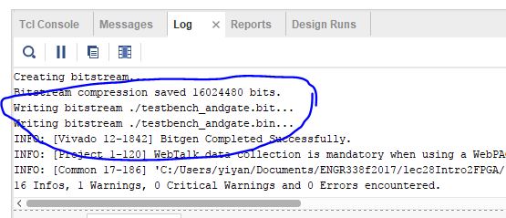
Generate Bitstream
Make
sure there are not errors, and both the .bit file and .bin file are
generated successfully. .bit file is used to program the FPGA from your
JTAG wire. If you power off your FPGA, all the program will be gone.
However, .bin file can be saved on an on-board memory, which can be
saved permanently until you flush if with another .bin file.
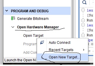
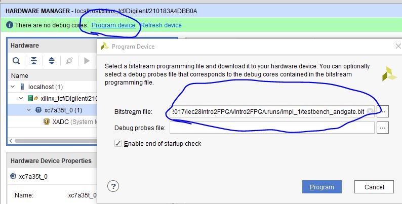
Open Hardware Manager, make sure your FPGA is connected to your
computer using a microUSB cable. Also, put the jump wire on the JTAG
spot (the jump wire position in the figure below is not correct for
programming from the computer, you need to move it one step down).
Go the navigation menu on the left, Open Hardware Manager:
Program the device
Now,
a tiny 'And Gate' is synthesized on your FPGA chip. Imagine how cool it
is. You will never need to use the bulky ICs to wire everything on the
breadboard. This single tiny chips can implement huge logic for you!
Try your sw[0] and sw[1] on the board as the inputs for the And Gate,
to control teh LED [0].
Before
we wrap up this lab, let's try to use the on-board memory to program
the chip instead of using your computer. If you power off your board,
the program will be gone. But the .bin file in the on-board memory can
be stored permanently.
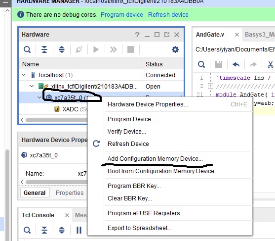
Pragram the chip using the on-board memory.
Right click your device in the Hardware window and select Add
Configuration Memory Device....
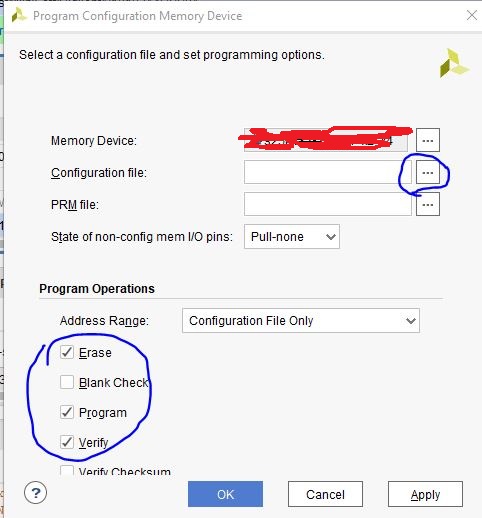
In the next window, type 'spansion' in the search engine, and select
the one that has 32 bits for the density
In the next window, select the .bin file you generated just now:
Then,
the on-board memory just received all your program .bin data. Now,
let's change the jump wire to QSPI, and push the push button 'PROG'
beside the jump wire on the board.
Now, you won't lose your logic if you power off the board.
1. When program the board using .bin file from the on-board memory, the
Jump Wire has to be set at the QSPI spot. Otherwise, nothing can be
programmed and the previous data will be flushed.
2. When program using the .bit file, the Jump Wire has to be at the
JTAG spot. (This may not be the case anymore for your Basys 3 board).
3. If the .bin file is updated, right click the memory device and
configure the file again.
Congratulations,
this simple 'And Gate' example for both Simulation and on-board
verification is done. You will be ready for a larger project using FPGA
in the future.
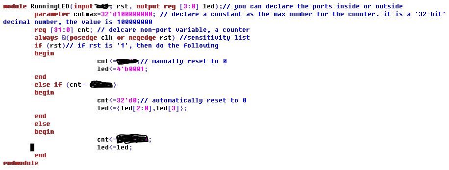
Running LEDs
The running LEDs demonstration video can be found in the following
video:
There is a 'reset' function to reset the LEDs to the original
state.
Hints for this program:
1) The timing for the running
led is controlled by the on-board oscillator (100 MHz). To convert it
to a 1 second timer, we need to count for 100 MEG times and then do
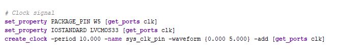
something. Before you code anything, make sure you enable the clock in
your constraint file.
2) The main body for the module can be:
I crossed out some of the parameters/variables in the program.
---------------------------------------- Tasks:
1. Implement the AndGate design to your FPGA board using switches as
inputs
and LEDs as outputs. Take pictures of all these four input combinations
and corresponding output LEDs. Include the snapshots in your
report. Use the same procedure to create XOR and OR
gates. (25 points) 2. Use both the volatile and nonvolatile methods (QSPI) to program your
FPGA (use the AndGate problem). Include the link to the video demo in your report. (10 points) 3.
Use Verilog and Vivado to demonstrate the following combinational
logic blocks in both simulation and on the FGPA board (switches/leds): (45 points)
1) 2-bit full adder 2) 8-input AND 3) 4-1 MUX
(can use an embedded condition: y=s1?(s0?d3:d2):(s0?d1:d0))
Note the Verilog conditional operator: (condition ? value_if_true :
value_if_false) 4. Similar
to the running LEDs example in the tutorial, show running LEDs on all
16 LEDs. It must have the reset function to restart the running LEDs
from the first LED. Include your code, testbench, and the link to a demo video in your report. (20 points) ---------------------------------- ** A summary on the
different
programming techiniques on the BASYS 3 board:
1. Jump wire to JTAG is to program the FPGA chip and the on-board
memory. So you need to do this first.
2. Keep the Jump Wire at JTAG, unplug the USB cable to power it off.
Then power it up again, the logic should disappear.
3.
Chage the Jump Wire from JTAG to QSPI, then press the Red Push Button
on the right 'PROG'. This will program the FPGA again and this won't
disappear after you power it off and back on.