The
VBP104S/SR photodiode does not output signals. I spent a few hours on
it but was not able to figure things out. This is not a very popular
photiode and there is very limited resources and examples online. Let's
switch to a visible photodiode that I have in my lab and use flash
light pulses to create voltage output from the amplifier PCB board.
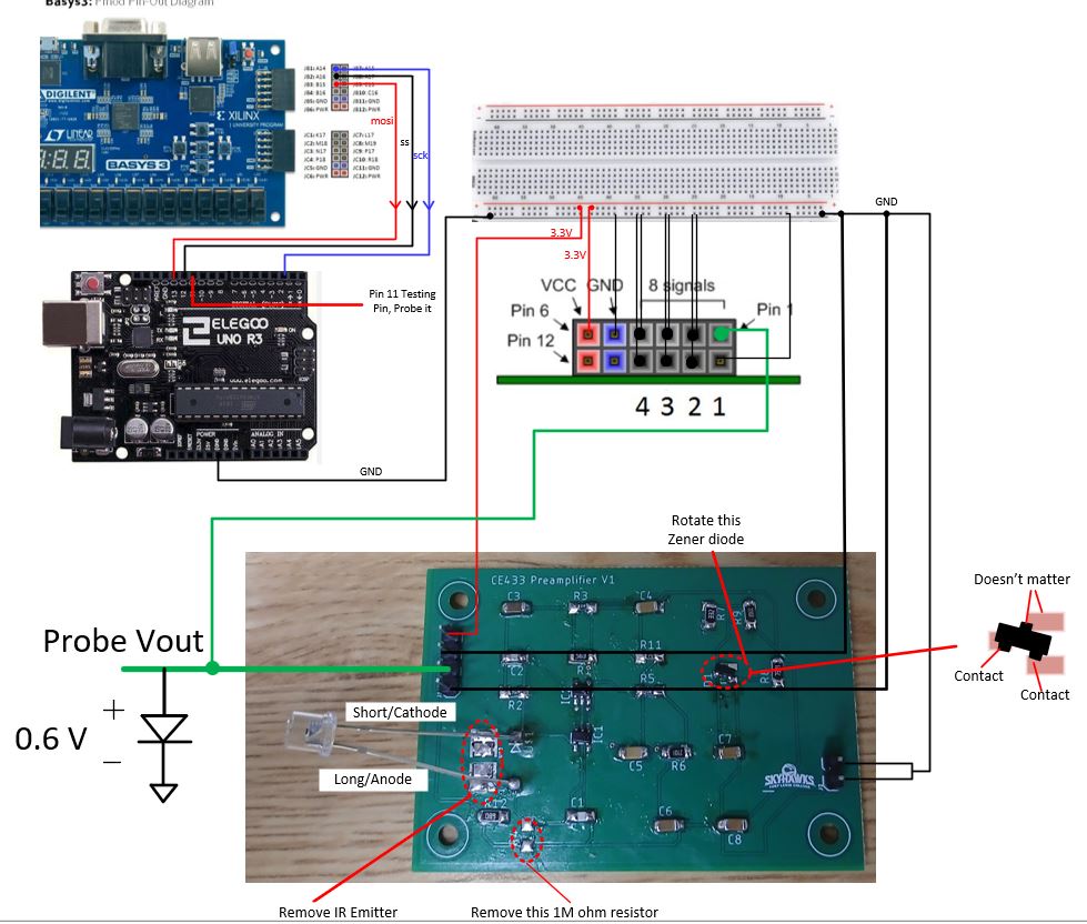
Here
is the new hardware connection that you need to complete at the
beginning of the lab. If you haven't soldered the PCB yet, please go
ahead and get that done first. You can test your PCB using a flash light. Probe Vout and you should see pulses on the oscilloscope.
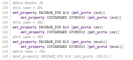
JB1 - 3 are used as sck, ss, and mosi respectfully.
The
FPGA board is now used as the leader transmitter, it outputs voltages
to the 5V logic Arduino so no level shifter is needed in this circuit.
On the Arduino board, Pin 13 is mosi, Pin 12 is ss, and Pin 2 is sck.
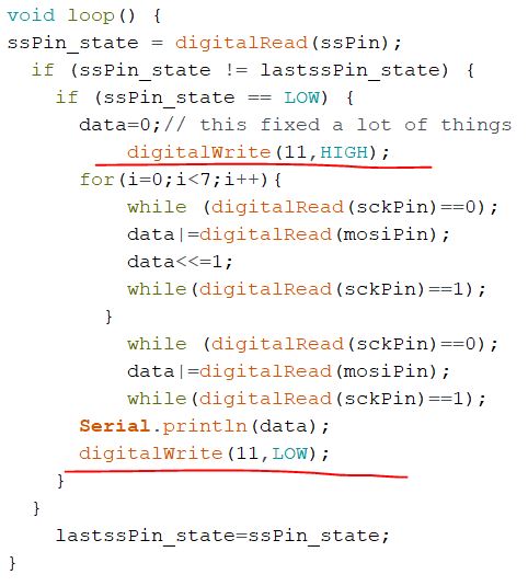
Pin
11 is used as a testing pin in your C code. This is a very handy
technique to debug your circuit. If you are taking my MCU class in the
fall, you will use this technique quite often.
This is how Pin 11 creates a pulse to indicate that this piece of code is executed.
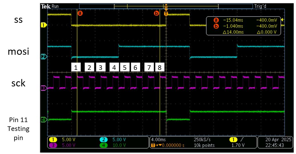
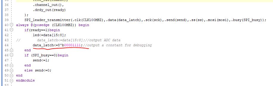
Here
is the observation. The mosi line comes from the FPGA. I wrote a
constant value 8'b00001111 to the mosi output from the FPGA for
debugging purposes.
In the SPI_leader_transmitter.v code,
at the negedge of the sck, ss is pulled down to 0 at the same time to
enable the follower device. From the observation above, at the left
handside of the label '1'. The falling edge of sck, mosi, and ss almost
happened at the same time. Waiting for a half sck cycle to sample the
data on the mosi line at the rising edge of the sck clock will be
perfect (the yellow cursor labeled '1' or 'a' samples a '0' from mosi).
The 'a' cursor samples a 0 from mosi, and this 0 is the MSB of the byte
'8'b00001111' sent through the FPGA.
After
sck rising edge No. 1, you can count to 8 sampled bits by Arduino
and the 8th rising edge is right before the 'ss' enable line got pulled
up to disable the transmission. This signals the completion of
transmission of 1 entire byte.
The Testing pin is pulled up and down at the correct time points which indicates that the Arduino code is executed as expected.
Observing
the output from the FPGA should be the first step of this project since
we need to know that the SPI leader transmitter module is functioning
before moving on.
I
connected the entire circuit to Arduino and looked at the output to the
Serial monitor. I received '15' constantly there so this is a great
news.(8'b00001111).