Week 7 Universal Asynchronous Receiver/Transmitter (UART)
1. Understand the UART protocol
Being asynchronous, the UART does not need a common clock between the
transmitter and receiver. Thus, connected devices can work
independently. The serial pin of the transmitter is generally called
transmit (TX). The corresponding receiver pin is generally called
receive (RX). The connection between the transmitter and receiver is
established by physically wiring these two pins.
The transmitter module will be basically a shift register that loads
parallel data and shifts it in a specific rate through TX pin of the
device. The receiver module will convert the received serial data
through RX pin into parallel form to be processed by the receiver.
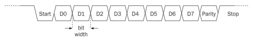
Data is transmitted in terms of packages in the UART. Data framing of a
UART package begins with a start bit, followed by seven to eight data
bits optionally attached by a parity bit (explained in Sec. 8.6), and
concluded by one or two stop bits.
as the transmission starts, the receiver should know the duration of
each pulse in the UART package. This is set by the baud rate which
determines the timing. The baud rate is denoted by bits per second
(bps). For example, a 2400-bps indicates a 416-µs bit width (or period)
in the UART transmission.
The TX pin should be at logic level 1 when the transmitter is in idle
mode. Once transmission starts, a falling edge is created on the data
transmit line which wakes up the receiver. Afterward, the clock is set
according to the baud rate and all bits are sent one by one in every
clock cycle in the transmitter side. The receiver should have the same
baud rate for receiving transmitted bits sequentially. As the transmit
operation finalizes, the TX pin should be set to logic level 1 for one
or two bit widths to informthe receiver that the transmission is done.
These are also called stop bit(s). The number of stop bits and usage of
parity bit should also be predetermined so that the transmitter and
receiver have same settings.
The data format is shown below:
Each device should have both the Receiving module and the Transmitting
module. The connection between two devices are RX - TX, and TX - RX.

If you don't have a textbook, please print out this PDF to study the UART protocol.
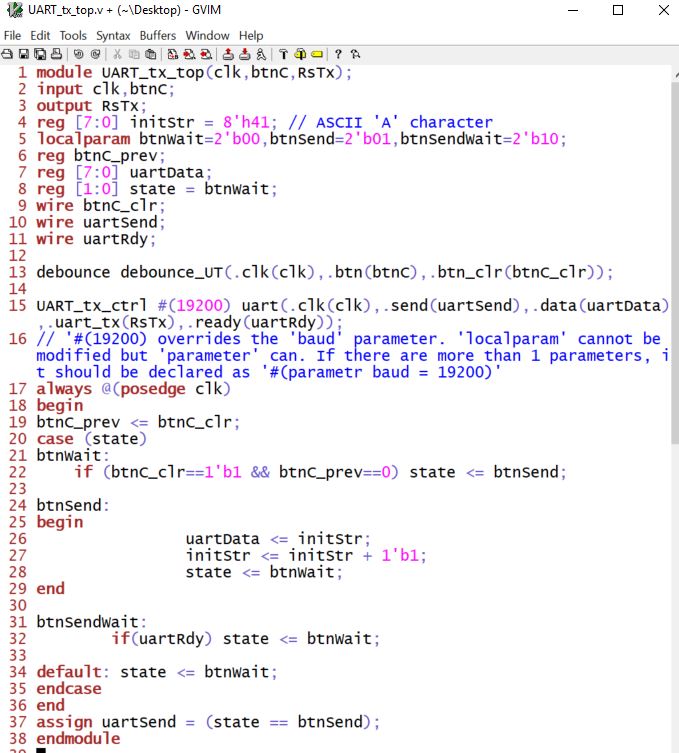
2. To implement the transmitter
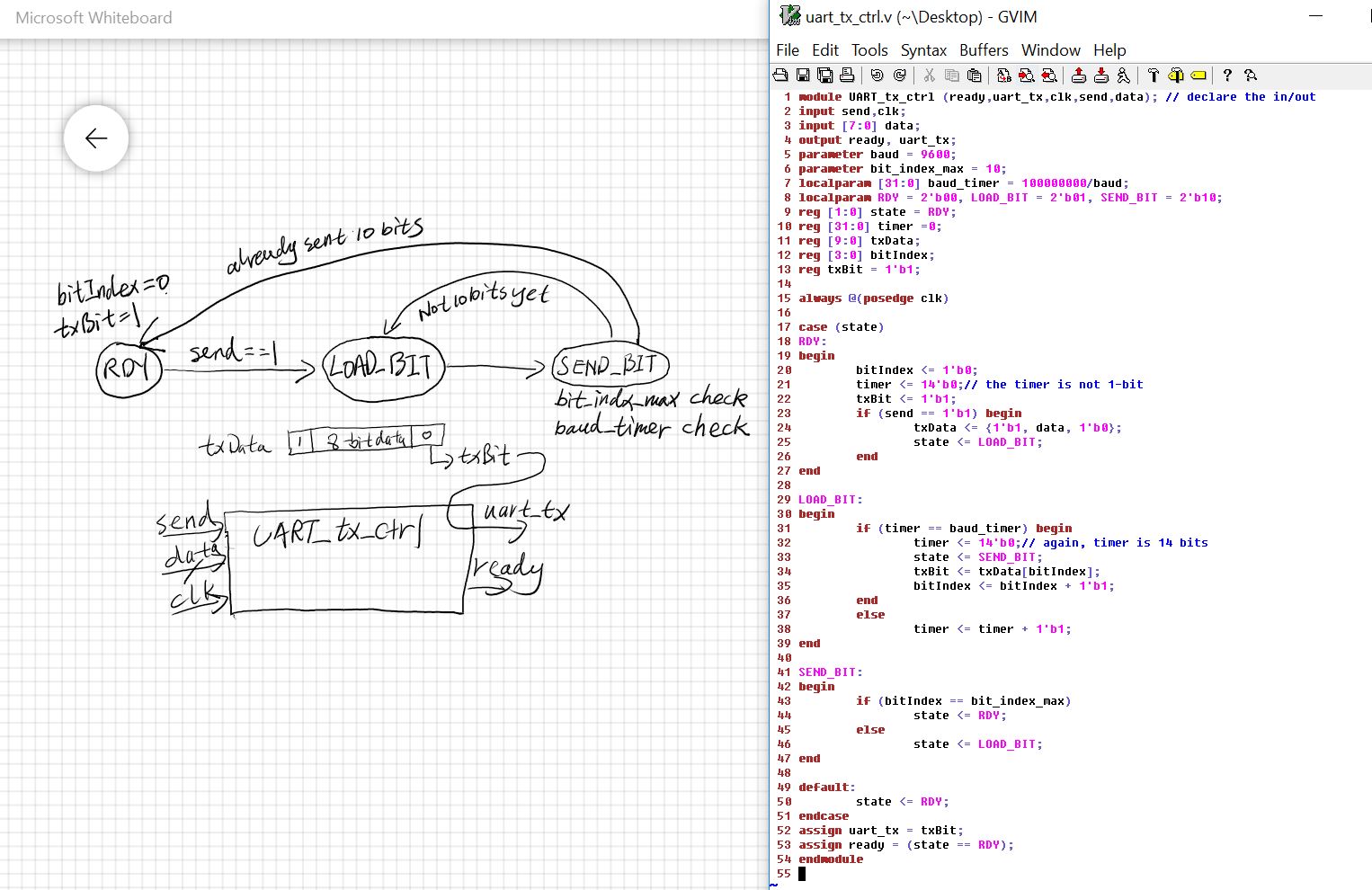
To implement a design in Verilog, you must design the FSM (Finite State Machie) first. In
practice, you don't have to draw all the details on the state diagram
at once. You can draw the critical states and transitions first, then
code it up in Verilog. Once the essential part of the Verilog code is
done, you can wrap it up by completing the signal declaration etc.
Keep in mind that nothing will be done until 'send ==1'. When the 10
bits are sent, it will come back to the RDY state to standby.
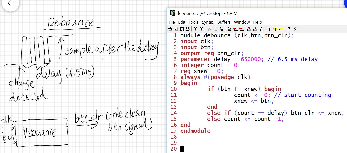
The debounce module in Verilog from listing 9.20 on Page 269.
The 650000 parameter creates a 6.5 ms delay because 650000 / 100 MHz =
6.5 ms. There is a little inaccurate information in the handdrawing
below. The 6.5 ms starts after the pulses. It waits for 6.5 ms after
there is no signal change.
The top level design:
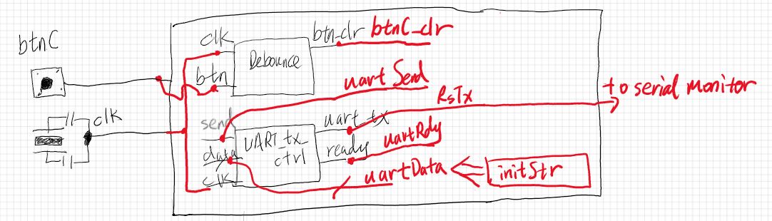
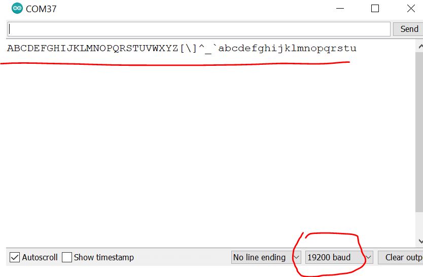
This top module will send ASCII code of letters/symbols to the Arduino serial monitor on a laptop/desktop.
In the script above, I don' tthink the 'btnSendwait' state is being
used. I think you can ignore that part. It didn't affect the result
because your pressing is way slower than the data transmission rate so
it is always ready to send the next byte.
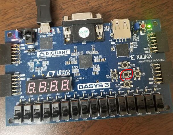
Keep pushing btnC, you will see all the ASCII code starts with letter A. (Use the Arduino serial monitor).
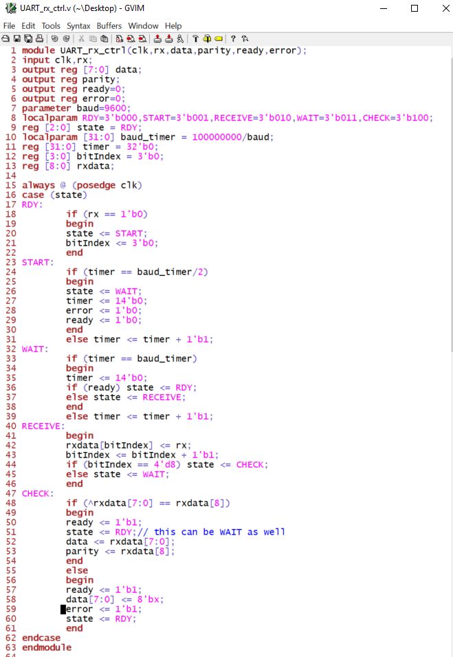
3. To implement the Receiver
The state diagram and the script.
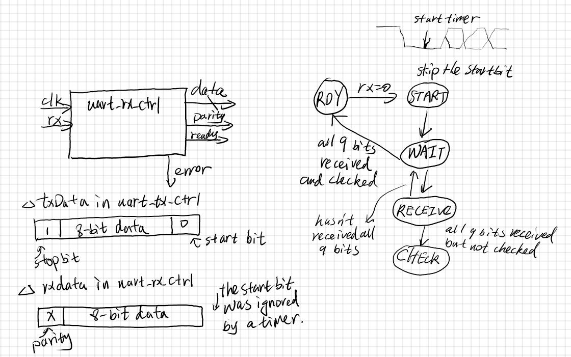
The 'START' state checks if it reaches baud_timer/2 because it is
trying to clear the timer and start the timer in the middle of the data
for sampling. Timer is cleared here so it always counts to baud_timer
when it is at the middle of the next bit.
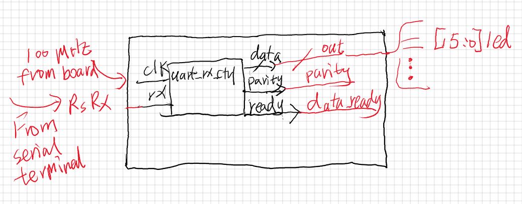
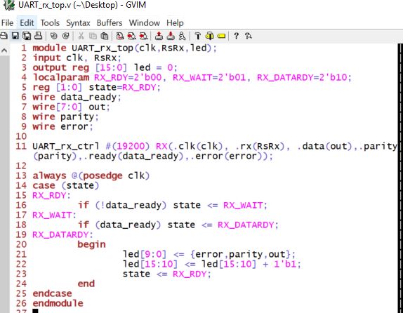
The top module:
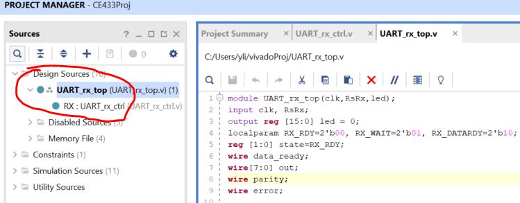
Remove the other files added to the project previously and add UART_rx_ctrl.v and UART_rx_top.v to the project.
Run the standard procedure:
Synthesis - Implementation - Gnerating Bitstreams - Open Hardware Manager - Program Device
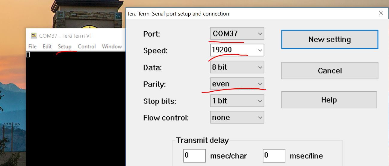
We need to set the parity to be Even Parity. The Arduino terminal
doesn't have this option for users so I switched to Tera Terminal.
Download the Tera Terminal from here:
https://ttssh2.osdn.jp/index.html.en
Making the following changes: Setup - Serial port
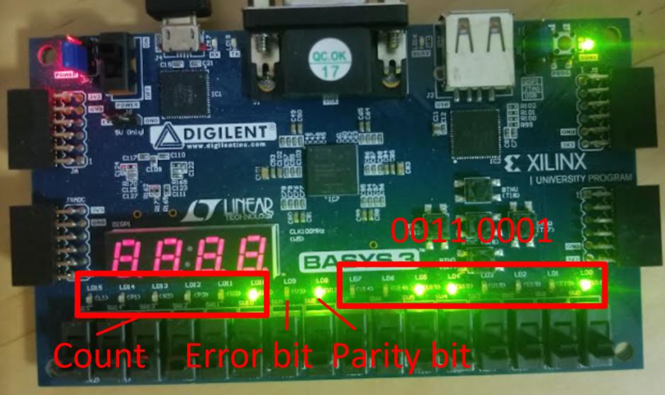
The received data is written to the first eight bits of led. The parity
bit is represented as the ninth led entry. If a transmission error
occurs, it is indicated in the tenth bit of led. Last six bits of led
are used to show how many packages have been received from the host PC.
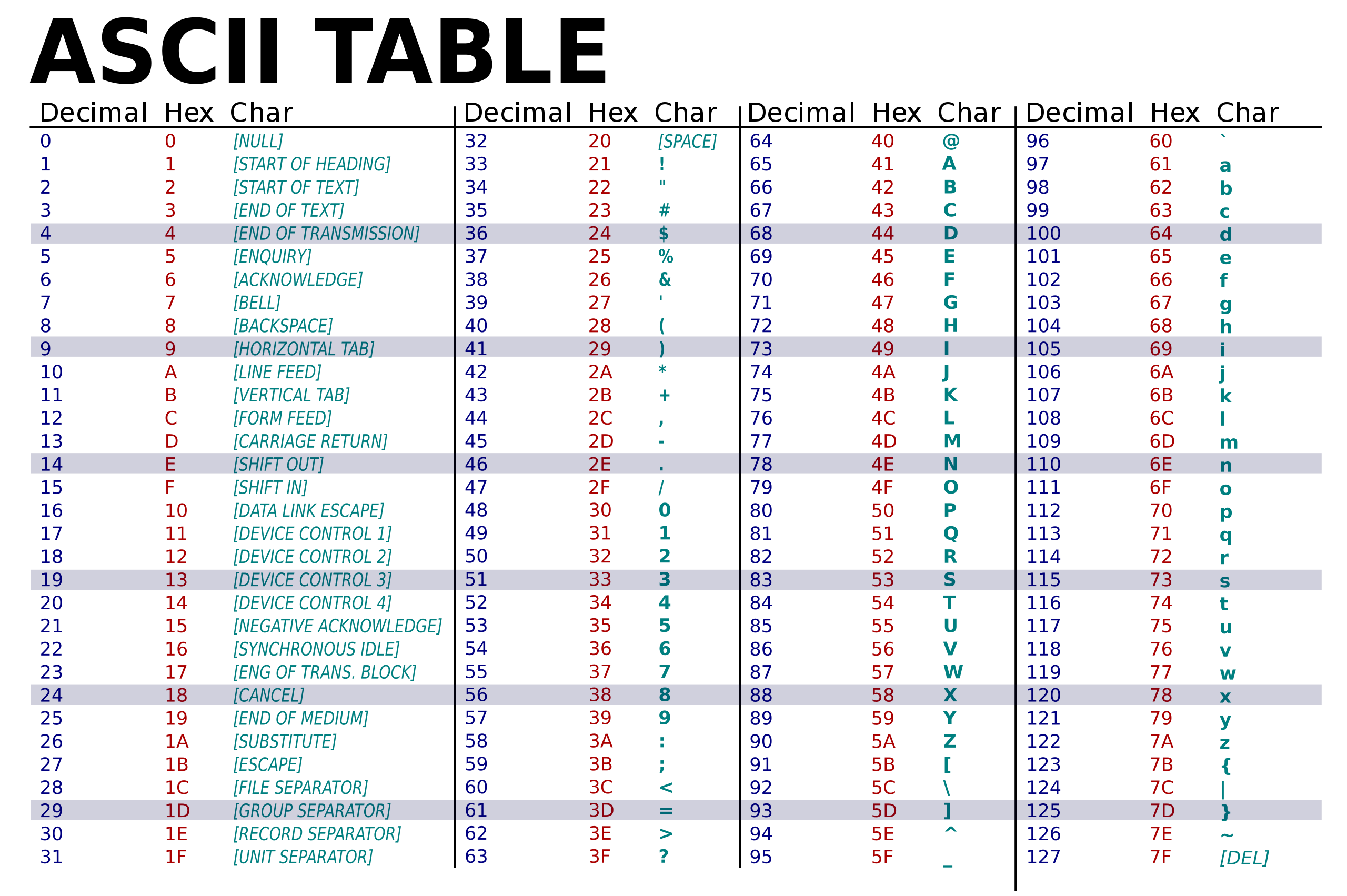
The ASCII table
The Character '1' is 49 (Dec) or 31 (Hex). Hex is easier to find - Ox31
is 0011 0001. I typed '1' in the terminal window and I got the
following LEDs lightened up on the board:
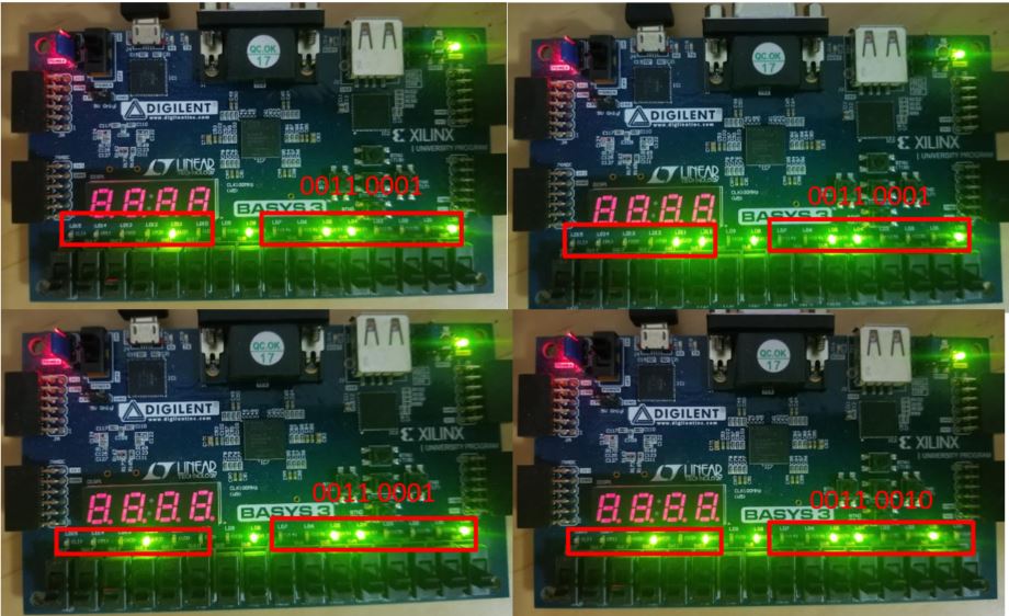
The ASCII code for '2' is 50 (Dec) or 32 (Hex), Ox32 is 0011 0010. I
typed 3 more '1's in the terminal and finally I typed a '2' there. I
received the following results which are what I expected.
-------------------------
Tasks:
1. In section 2. use the debounce module to create a counter. When the
user press the button once, it shows a '1' on the seven segment
display. If the user keep pushing the button, the display increments by
1 until 9 then it resets to 0.(25 points)
2. Repeat the UART transmitter in Section 2 to show letters/symbols in the serial monitor. (25 points)
3. Repeat the work in Section 3. (25 points)
4. Show the numbers you typed in the
serial monitor on one seven segment display unit (less than 10).
(25 points)