Week 5 Sequential Circuit
1. State and Output Equations
To represent the output of a sequential circuit, we can use two
different models as Mealy and Moore. In Mealy model, the output is a
function of both present state and input. In Moore model, the output is
a function of the present state only.
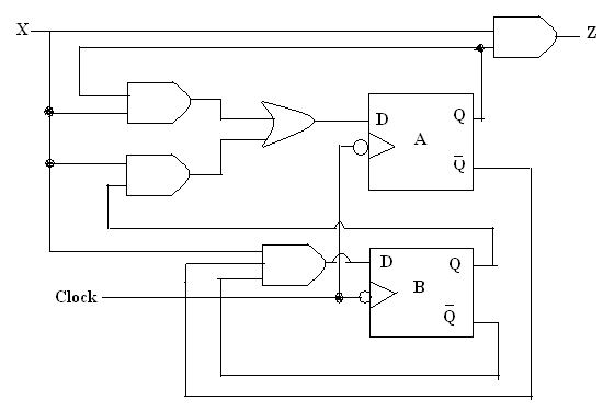
An example:
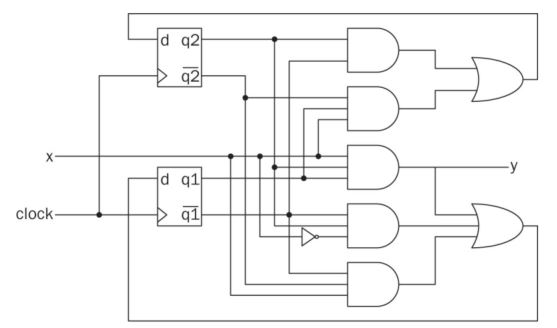
From the circuit above, we can find the following logic equations:
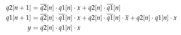
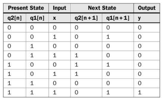
From the equations, we can find the state table.
Now let's recap the process of converting a state table into a sequential circuit:
You can follow the same process to find q1(n+1) and y.
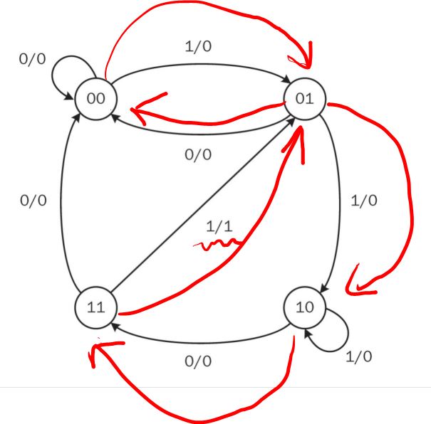
2. State Diagrams
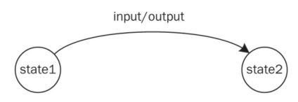
If the sequential circuit is of the Mealy type, the directed arc holds
what the corresponding output will be after the state transition.
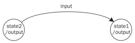
The state diagram based on the Moore model requires outputs to be
defined along with states. As can be seen in this figure, the directed
arc only contains the input value required for transition. The circle
representing the state also holds the corresponding output value.
The table in Section 1 is definitely a Mealy model. The state diagram
is as follows:
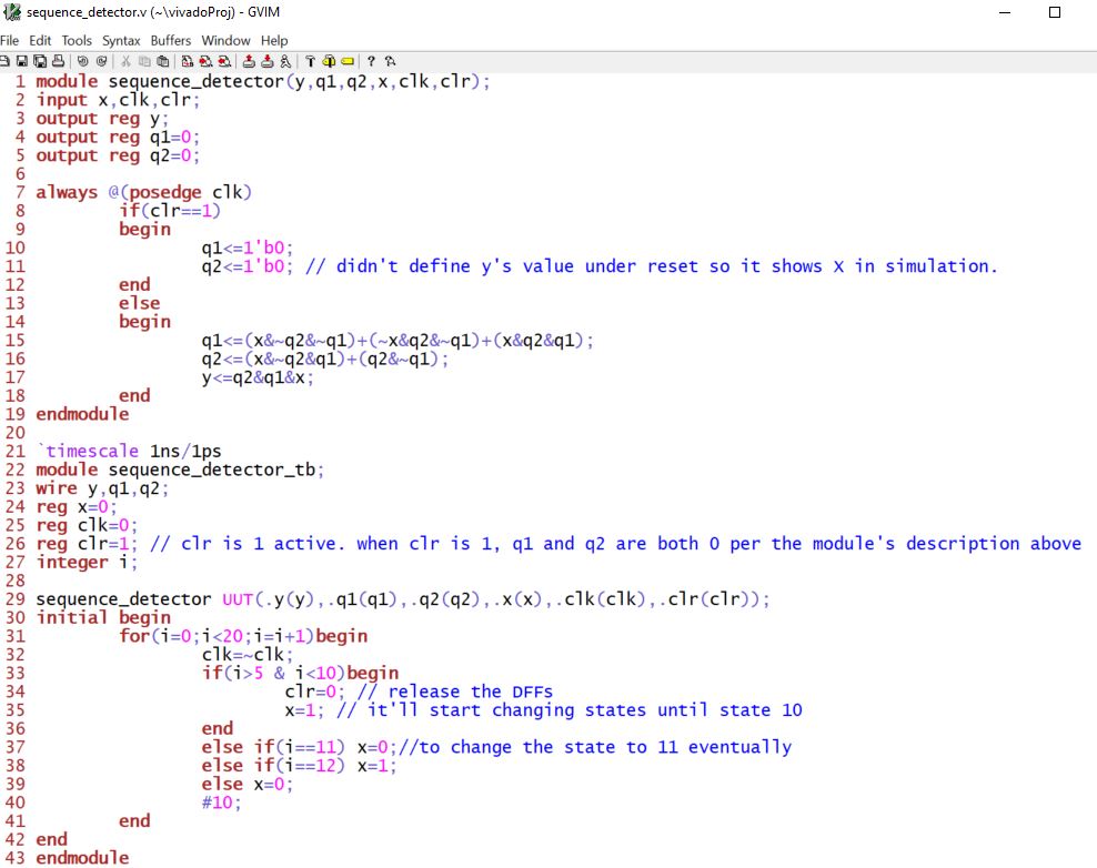
3. Verilog implementation
Using the logic equations
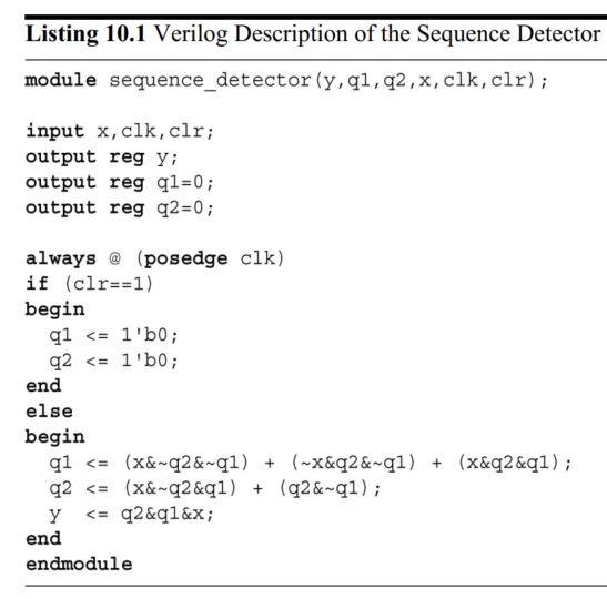
Verilog implementation
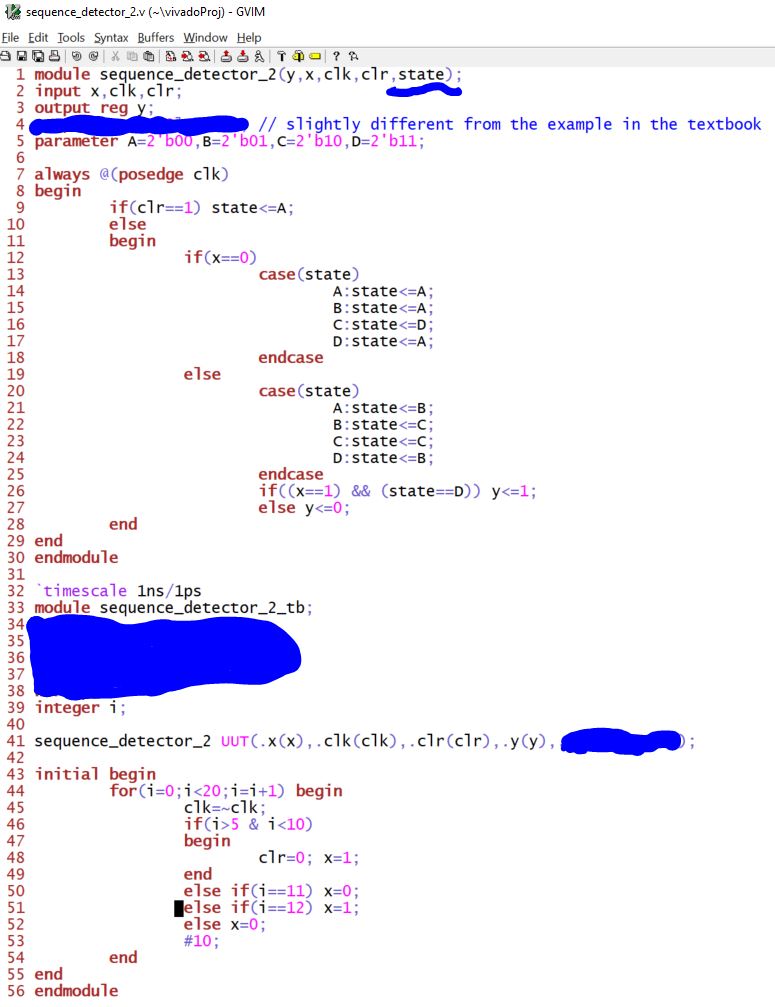
When I wrote the
testbench, I referred to the state diagram to find the logic states
that I would like to verify. However, it didn't go through all
possibilities in the state diagram. You can modify the testbench to
verify all possibilities or you can run multiple simulations to verify
different paths in the state diagram.
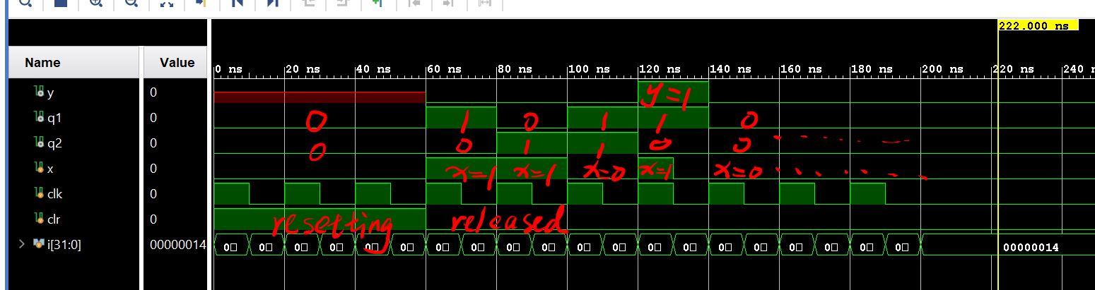
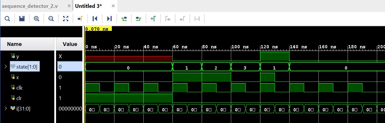
The simulation results verified the following paths in the state diagram:
The rising edge of the clock is able to detect the signal change at the
rising edge of X and change the state. For example at time 60ns, the
rising edge detects X=1 and changed the state to q2q1 = 01, y=0.
Using the behavioral form
The behavioral form is nothing but a summary
of the state diagram. You must include all possibilities that covered
by the state diagram.
Verilog script/testbench and simulation results (it shows the same simulation results to the last one.
Since we are going to test it
so the 2-bit state pins should be made available for external use. The
'state' pin is declared in the module and wires are connected to the
two pins from the testbench. I masked part of my script for you to fill
in.
4. Timing in sequential circuits
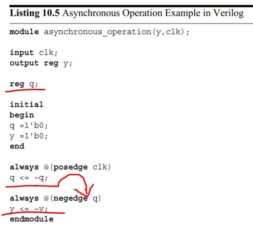
Synchronous Operation
The description under always @ (posedge clk) is responsible for state
transitions and output formation. The posedge keyword indicates that
the always block is executed whenever a rising edge of clock comes.
Asynchronous Operation
5. Shift Registers
The family of devices performing this operation is called shift
register. There are four shift register types: serial in/serial out,
parallel in/serial out, parallel in/parallel out, and serial
in/parallel out.
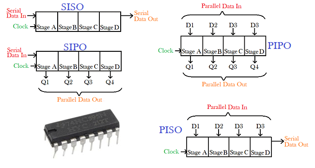
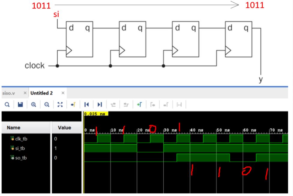
Take the SISO one as a example. The circuti diagram:
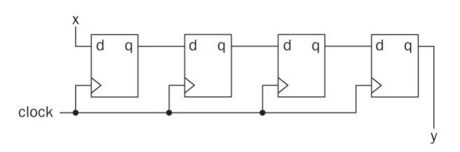
Here, each bit in the sequence to be shifted is saved in a flip-flop
named qi. In this setup, let q0 and qN−1 represent the least and most
significant bits, respectively. This shift register can be explained
best using its state and output equations as follows:
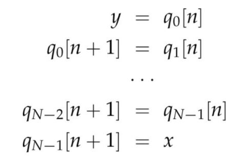
As can be seen in above state equations, at every clock bits are
shifted to the right flipflop. The output equation indicates this is a
Moore machine since the output depends only on the present state value.
Verilog has predefined operators for shifting data in a vector. The
shift right operator is “>>”. The shift left operator is
“<<”. Let’s assume that a vector Q is to be shifted to left by
one bit. The Verilog description for this operation will be Q <<
1.
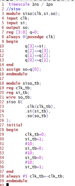
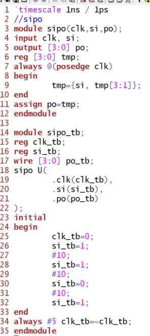
Implement SISO in Verilog: (including the testbench)
The simulation results:
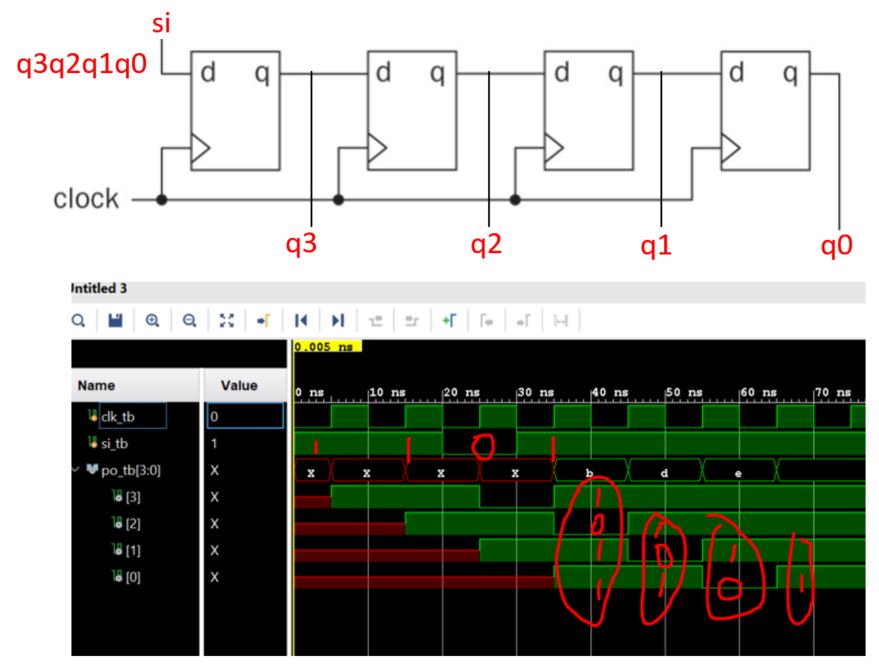
Implement a right shift SIPO in Verilog (including the testbench):
The simulation results:
PISO (parallel in serial out):
Implement it in Verilog:
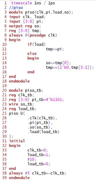
The simulation results:
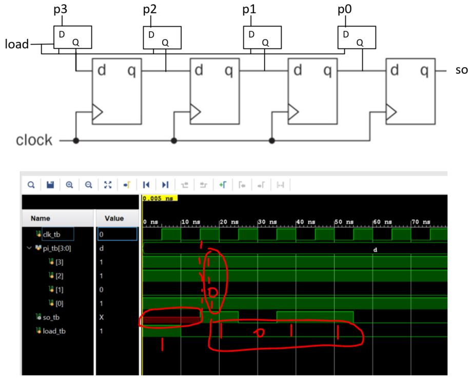
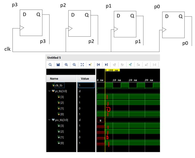
To implement PIPO in Verilog (including the testbench):
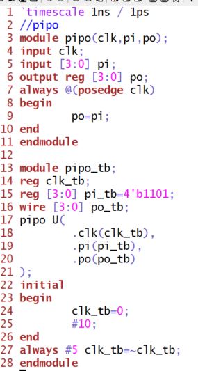
The simulation results:
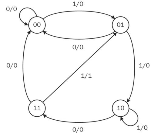
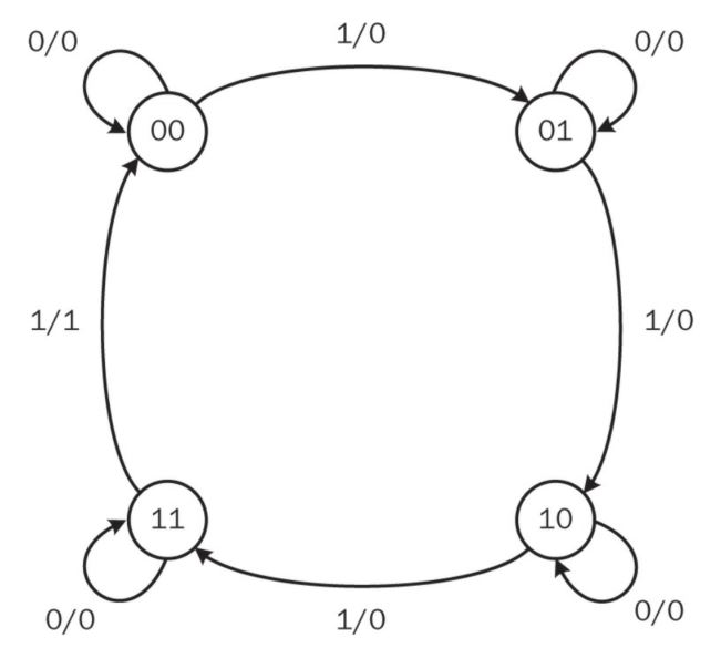
6. Counter as a Sequential Circuit
The counter can best be
explained by its state diagram. Let’s pick a two-bit (four state) up
counter as example. States of this circuit will be 00, 01, 10, and 11.
Hence, the circuit will count upwards. If the count value reaches state
11, then the next state will be 00. To indicate that the count reached
the final value and restarted counting, we can set the output as logic
level 1 at this transition.
A counter can be realized in two different ways as a synchronous or an asynchronous sequential circuit.
6.1 Synchronous counter
In a synchronous counter, all flip-flops within the sequential circuit are clocked with the same clock signal.
The state and output equations:
The sequential circuit of the 2-bit synchronous up counter:
In Verilog: (Please keep in mind that the {y,q}<=q+1'b1 assignment doesn't work!!! You must revise it as {y,q}<={y,q}+1'b1)
An N-bit synchronous up/down counter with the 'clear' function.
6.2 Asynchronous counter
There is another way of
implementing the two-bit up counter. To do so, we should analyze the
state table more closely. As can be seen in this table, q1 toggles its
state whenever rising edge of clock comes and input x equals to logic
level 1. q2 toggles its state whenever falling edge of q1 comes and
input x equals to logic level 1. This leads to asynchronous (ripple)
counter in which clock signal is fed only to the first flip-flop. The
second flip-flop changes its state based on the output of the first
flip-flop.
7. Frequency division
The clock frequency of a
digital system may not be suitable for operation. Hence, we may need to
change it. Module performing this is called frequency divider. Counters
can be used for this purpose. What we have to do is feeding the clock
signal as inputand obtaining new clock signal with the frequency
divided by powers of two from the output of counter flip-flops.
Here, we use T (toggle) flip-flops
--------------------------------------
Tasks
1. In Section 1, don't look at the logic equations provided to you.
From the state table, find the logic equations for q1(n+1) and y and
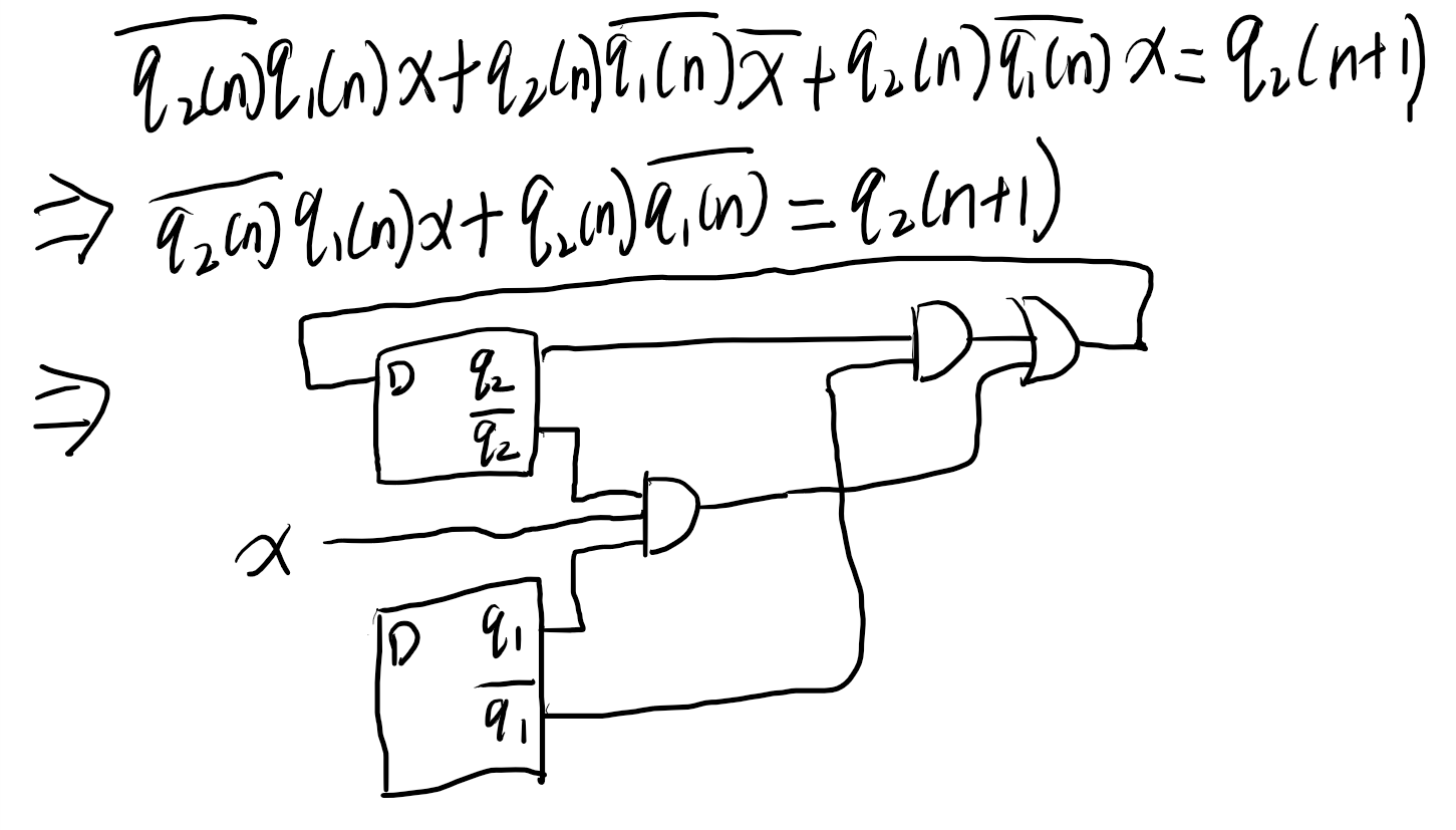
draw the sequential circuit for q1(n+1) and y. (10 points)
2. Repeat the work in Section 3. Use two methods, the given one and the behavioral one. Show simulation results. (15 points)
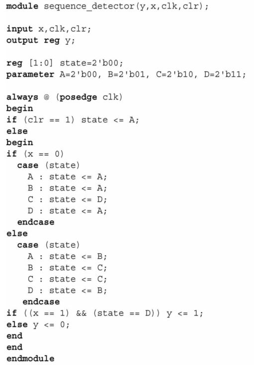
3. Similar to the sequence
detector in Section 3, change the sequence to be detected to 1011,
design the state diagram, draw the truth table, find the logic
equations, and design the verilog module and testbench to verify the
logic. (15 points)
4. Simulate the four types of shift registers in Section 5. (20 points)
5. Build a counter module and show the simulation results. (20 points)
6. Find the logic equation of the following circuit and implement it in verilog. Show the simulation results. (20 points)