Week 3 Combinational Logic Blocks
1. Adder
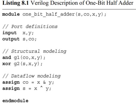
One-bit half adder:
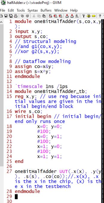
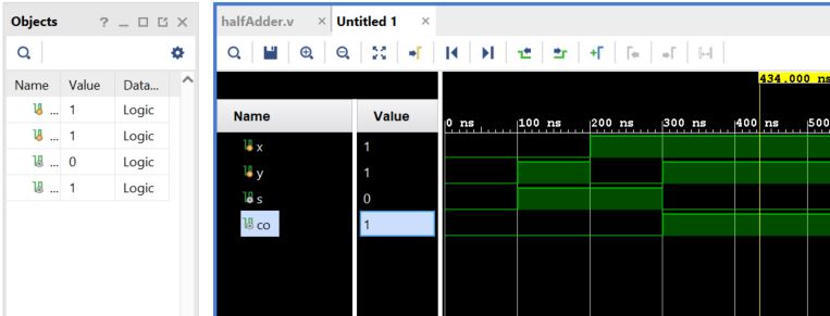
Vivado simulation (including testbench)
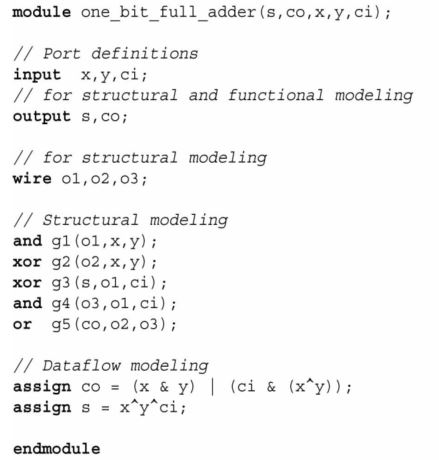
One-bit full adder
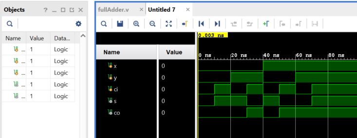
Vivado simulation:
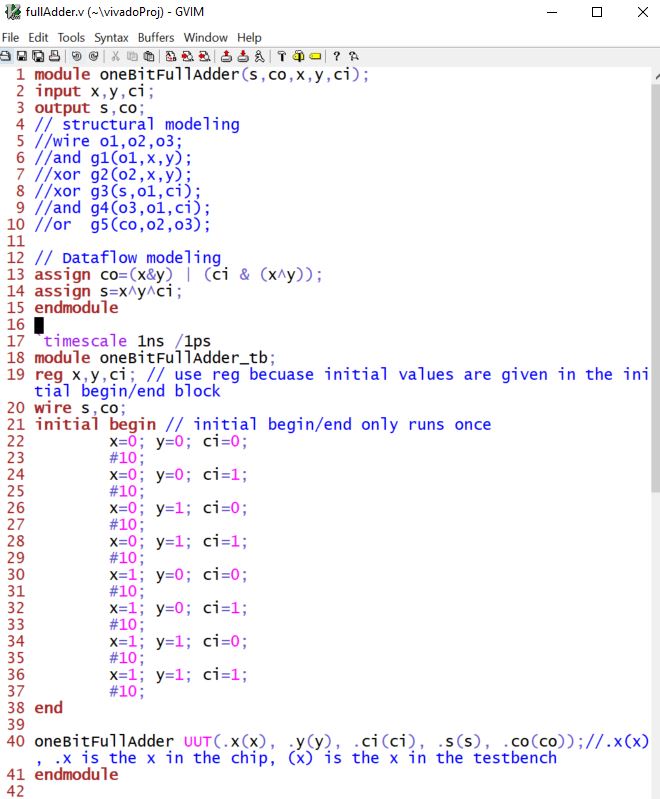
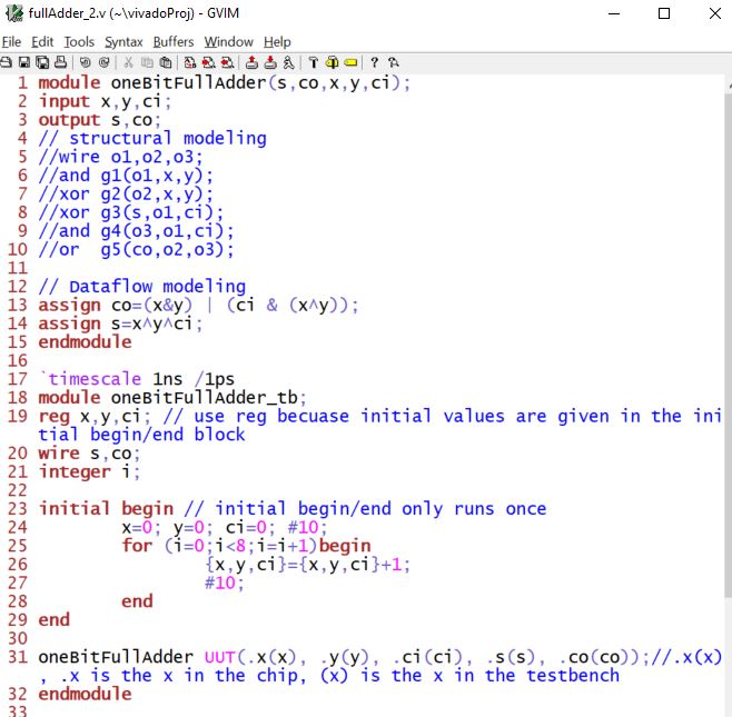
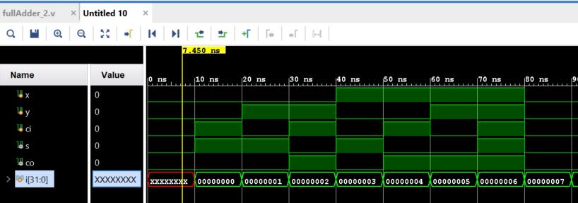
In the full adder testbench, when there are many simulation entries, you can use a for loop to simplify it.
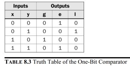
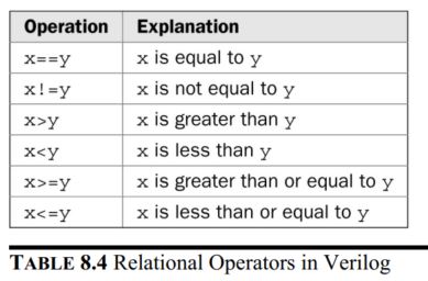
2. Comparators
We may need to compare the magnitude of two binary numbers to obtain
their status. Here, the first number may be greater than the second.
The two numbers may be equal. Or, the first number may be less than the
second. To achieve this goal, we will need a comparator. We can explain
the comparison operation on two binary variables x and y (each being
one bit) using the truth table presented in the following truth table.
Here, g, e, and l stand for greater, equal, and less, respectively.
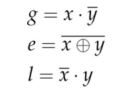
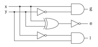
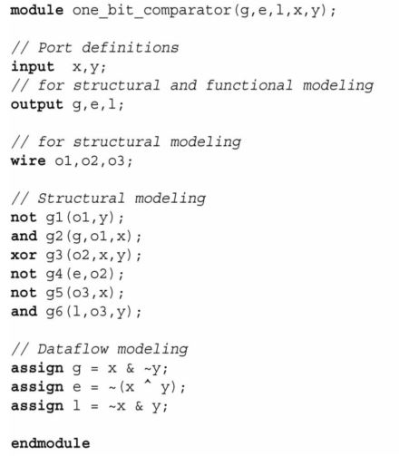
In Verilog:
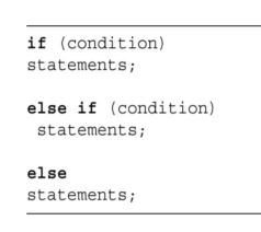
3. Conditional statement in Verilog
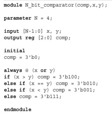
A 4-bit comparator
An N-bit comparator can be constructed by the 'if' keyword. Here, two
vectors each with four-bits (x and y) are compared and the result is
written to another vector comp. If the first vector is greater than the
second one, then comp[2]=1. If the second vector is greater than the
first one, then comp[0]=1. Finally, if the two vectors are equal, then
comp[1]=1.
Another example of the IF Statement (not a comparator):
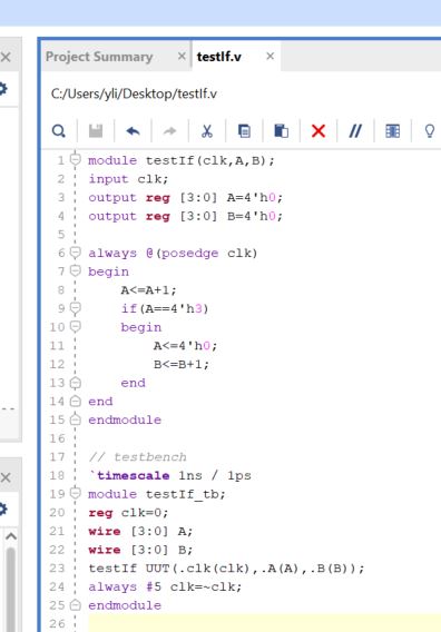
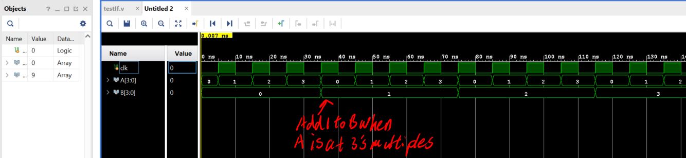
If I remove the 'begin/end' statement in the IF statement and keep
'B<=B+1' below the 'A<=4'h0' line, B will have an increment of 1
at each cycle.
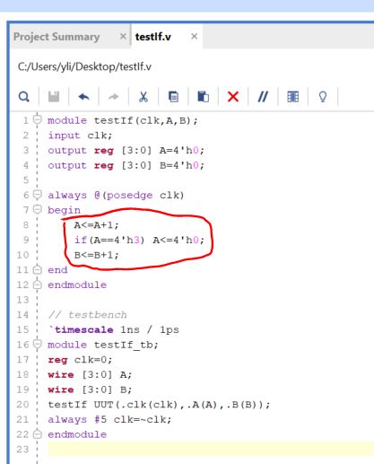
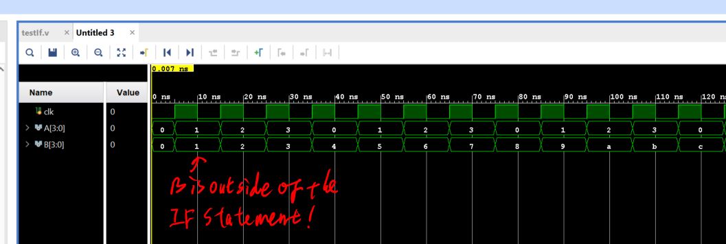
This example tells you that the 'begin/end' block defines the boundary of the IF statement if you have multiple lines there.
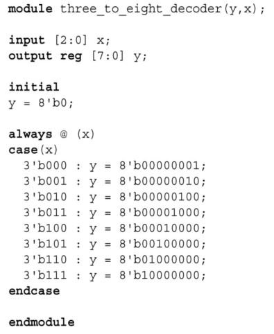
4. Decoders
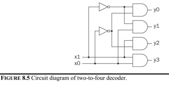
In Verilog,
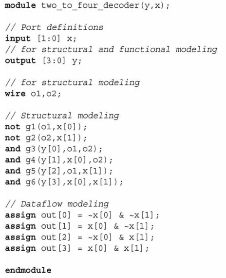
The 'case' statement
5. Encoders
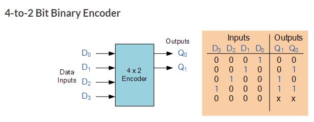
One of the main disadvantages of standard digital encoders is that
they can generate the wrong output code when there is more than one
input present at logic level “1”. For example, if we make inputs D1 and
D2 HIGH at logic “1” both at the same time, the resulting output is
neither at “01” or at “10” but will be at “11” which is an output
binary number that is different to the actual input present. Also, an
output code of all logic “0”s can be generated when all of its inputs
are at “0” OR when input D0 is equal to one. One simple way to overcome
this problem is to “Prioritise” the level of each input pin. So if
there is more than one input at logic level “1” at the same time, the
actual output code would only correspond to the input with the highest
designated priority. Then this type of digital encoder is known
commonly as a Priority Encoder or P-encoder for short.
Priority encoders
The Priority Encoder solves the problems mentioned above by allocating
a priority level to each input. The priority encoders output
corresponds to the currently active input which has the highest
priority. So when an input with a higher priority is present, all other
inputs with a lower priority will be ignored. The priority encoder
comes in many different forms with an example of an 8-input priority
encoder along with its truth table shown below.
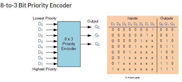
Priority encoders output the highest order input first for example, if
input lines “D2“, “D3” and “D5” are applied simultaneously the output
code would be for input “D5” (“101”) as this has the highest order out
of the 3 inputs. Once input “D5” had been removed the next highest
output code would be for input “D3” (“011”), and so on. The truth table
for a 8-to-3 bit priority encoder is given as:
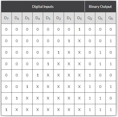
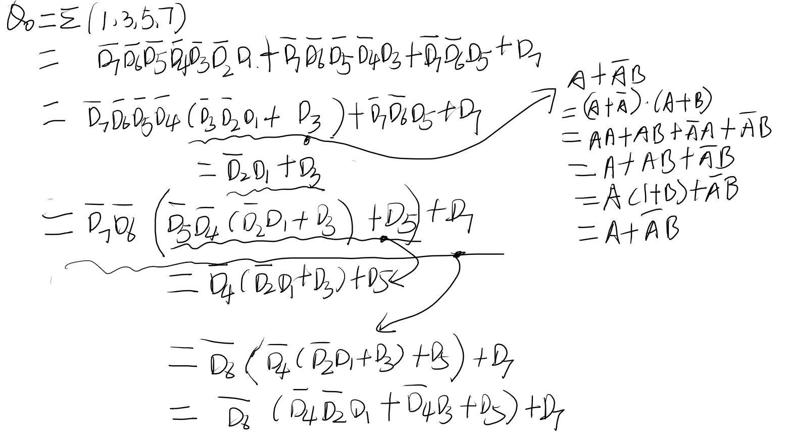
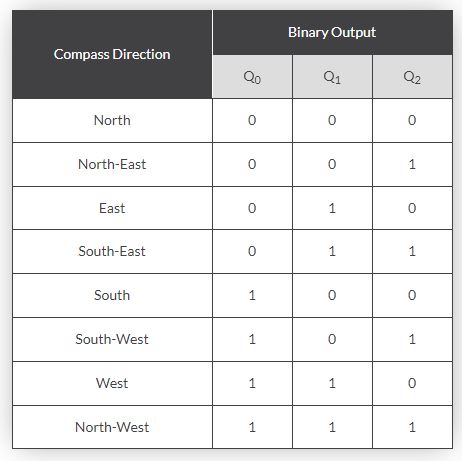
What are Q1 and Q2?
Digital Encoder Applications Keyboard Encoder Priority encoders can be
used to reduce the number of wires needed in a particular circuits or
application that have multiple inputs. For example, assume that a
microcomputer needs to read the 104 keys of a standard QWERTY keyboard
where only one key would be pressed either “HIGH” or “LOW” at any one
time.
One way would be to connect all 104 wires from the individual keys on
the keyboard directly to the computers input but this would be
impractical for a small home PC. Another alternative and better way
would be to interface the keyboard to the PC using a priority encoder.
The 104 individual buttons or keys could be encoded into a standard
ASCII code of only 7-bits (0 to 127 decimal) to represent each key or
character of the keyboard and then input as a much smaller 7-bit B.C.D
code directly to the computer. Keypad encoders such as the 74C923
20-key encoder are available to do just that.
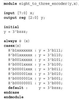
Verilog implementation using the casex statement:
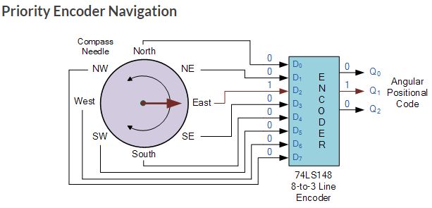
Positional Encoders
Another more common application is in magnetic positional control as
used on ships navigation or for robotic arm positioning etc. Here for
example, the angular or rotary position of a compass is converted into
a digital code by a 74LS148 8-to-3 line priority encoder and input to
the systems computer to provide navigational data and an example of a
simple 8 position to 3-bit output compass encoder is shown below.
Magnets and reed switches could be used at each compass point to
indicate the needles angular position.
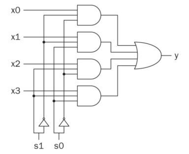
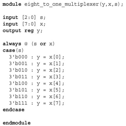
6. Multiplexers
An eight-to-one multiplexer
In Verilog
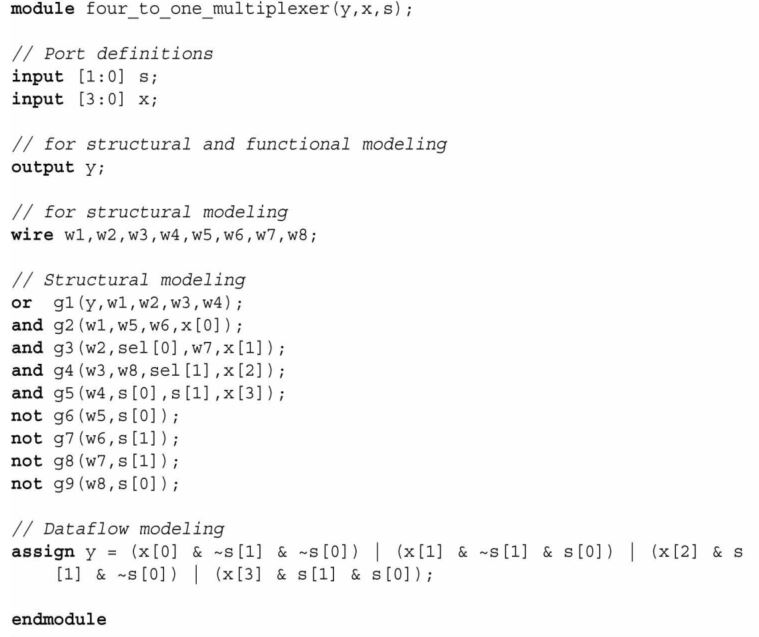
The 'case' version.
7. Parity generators and checkers
While transferring or storing binary data, some bit values may change
because of a physical effect or an unpredicted disturbance. To check
whether such an undesired change has occurred or not, extra bits can be
added to the data. This is called parity generation. The idea here is
setting standard characteristics to data such that when a change
occurs, it can be detected easily.
Even Parity Generator - The total number of 1's in input and the parity bit are even
Odd Parity Generator - The total number of 1's in input and the parity bit are odd
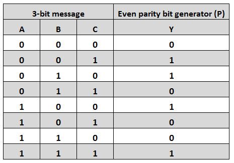
Even Parity Generator (make the total number of 1's even)
Let us assume that a 3-bit message is to be transmitted with an even
parity bit. Let the three inputs A, B and C are applied to the circuit
and output bit is the parity bit P. The total number of 1s must be
even, to generate the even parity bit P. The figure below shows the
truth table of even parity generator in which 1 is placed as parity bit in order to make all 1s as even when the number of 1s in the truth table is odd.
Use a K Map to find the logic expression of the truth table:
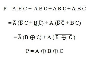
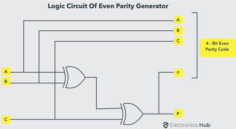
The above expression can be implemented by using two XOR gates. The
logic diagram of even parity generator with two XOR gates is shown
below. The three bit message along with the parity generated by this
circuit which is transmitted to the receiving end where parity checker
circuit checks whether any error is present or not.
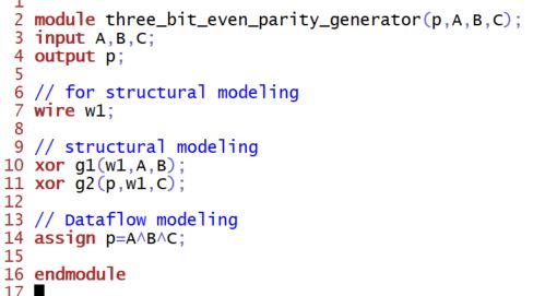
In Verilog:
Even Parity Checker
It is a logic circuit that checks for possible errors in the
transmission. This circuit can be an even parity checker or odd parity
checker depending on the type of parity generated at the transmission
end. When this circuit is used as even parity checker, the number of
input bits must always be even.
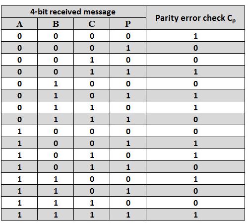
Even Parity Checker Consider that three input message along with even
parity bit is generated at the transmitting end. These 4 bits are
applied as input to the parity checker circuit, which checks the
possibility of error on the data. Since the data is transmitted with
even parity, four bits received at circuit must have an even number of
1s. If any error occurs, the received message consists of odd number of
1s. The output of the parity checker is denoted by PEC (Parity Error
Check). The below table shows the truth table for the Even Parity
Checker in which PEC = 1 if the error occurs, i.e., the four bits
received have odd number of 1s and PEC = 0 if no error occurs, i.e., if
the 4-bit message has even number of 1s.
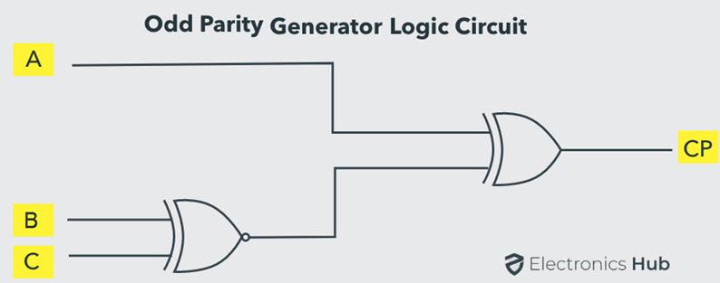
Odd Parity Generator (make the total number of 1's odd)
Truth table:
Logic expression:

Circuit:
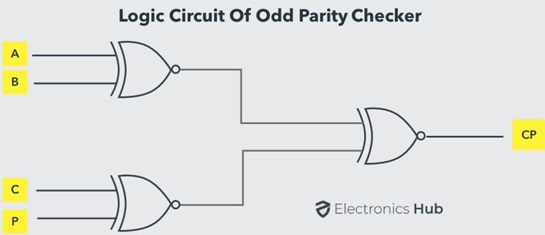
Odd Parity Checker
Logic expression:

The circuit:
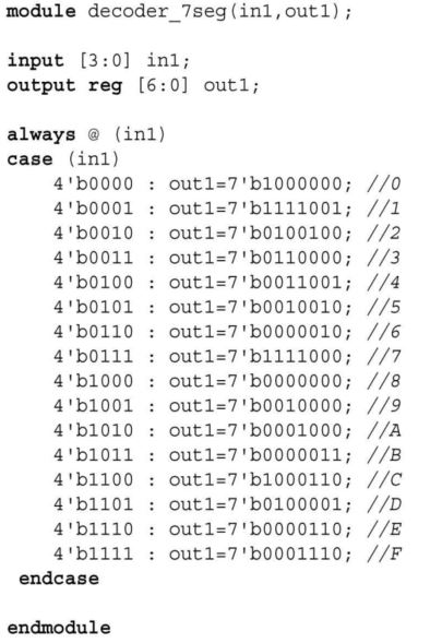
8. Improving the home alarm system
We can improve the home alarm system using a seven-segment display.
When the system is active, the display will show character A. When it
is closed, the display will show character O.
To do so, we should add a seven-segment display decoder module to the
system. This module converts the provided hexadecimal number to the
corresponding seven-segment display pattern.
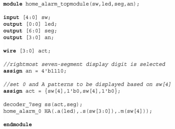
Please refer to the last tutorial to implement the improved home alarm system on your Basys3 Board.
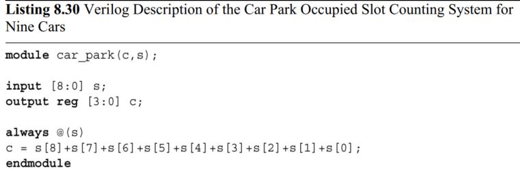
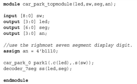
9. Improved car parking spot counting system
--------------------
Tasks
1. Repeat the simulation of Half Adder and Full Adder in Section 1. (10 points)
2. Design the testbench for the comparator in Section 2 and show the simulation results. (10 points)
3. Design the testbench for the 4-bit comparator in Section 3 and show the simulation results. (10 points)
4. Implement a 2-bit comparator on the Basys 3 board. Use sw as inputs and led as outputs. (10 points)
5. In Section 4, design the testbench for the decoder and verify the logic in simulation (use the Dataflow modeling method). (10 points)
6. In Section 5, for the 8x3 priority encoder, find Q2 and Q1, build the module and verify the logic using simulations. (10 points)
7. In Section 6, implement a 4-1 multiplexer on your Basys 3 board. Show embedded Youtube video demonstration on your report. (10 points)
8. Design/verify an even
parity generator and checker in simulation respectively. Implement an
even parity checker on your Basys 3 board - use sw as inputs, use leds
as output indicators. Show embedded Youtube video demonstration on your
report.(10 points)
9. Implement the design in Section 8 and Section 9 on your Basys 3
board. Show embedded Youtube video demonstration on your report.(20 points)