Different from the UART, the
SPI is a synchronous communication
protocol. Besides, communication between the transmitter and receiver
is duplex. In other words, data is transmitted and received at the same
time in the SPI. Therefore, the SPI communication uses four wires. Two
of these wires are for data transfer. One wire is used for the common
clock signal (for synchronization). The fourth wire is used to enable
(select) signal
Different from the UART, data
packet size is not constant in the SPI.
This is an advantage since the user can select the packet size as he or
she desires. Moreover, the dedicated common clock and enable signals
avoid using start and stop bits in the UART. The only requirement here
is the need for determining the data packet size. Hence, the
transmitter and receiver can understand each other.
SCK is generated by the
leader and fed to the follower
Here, SCK depends on the
maximum data rate of the transmitter and
receiver. Hence, the device with the lowest rate defines its limit.
Besides frequency, the leader also adjusts the polarity and phase of
clock denoted by CPOL and CPHA, respectively. Four possible
combinations of CPOL and CPHA are presented in the following figure.
These combinations are called modes of the SPI.
Transmission and Reception
Operations
In the SPI, the data
transmission and reception is controlled by the
leader through SCK and signals. When there is no transmission, stays at
logic level 1 and SCK stays either at logic level 0 or 1 depending on
the SPI mode.
The SPI communication starts
when the leader wakes the follower by
setting to logic level 0. Next, the leader and follower start
interchanging data in every clock cycle set by SCK. Here, either the
leader sends a bit through MOSI line or the follower sends a bit
through MISO line. The SPI mode also determines if data will be sent on
the rising or falling edge of SCK. After all bits are transferred, the
common clock stops and leader deselects the follower by changing to
logic level 1.
Read this PDF from the textbook to understand
the operation of SPI.
MOSI: The MOSI of the leader and
the follower: Leader transmitter:
Leader transmitter and follower receiver:
MISO: The MISO of the leader and
the follower:
Follower transmitter and leader receiver:
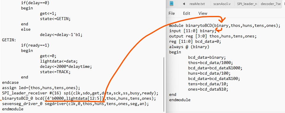
Line 18 for the
SPI_leader_receiver module, I used 8'd25 instead of 24 in the textbook.
2. SPI
Application - the PmodALS ambient light sensor
The
Pmod ALS (Ambient Light Sensor) by Digilent is named based on its
functionality and form factor: "Pmod" stands for Peripheral Module, an
open-standard interface designed by Digilent for connecting small I/O
modules to FPGA/microcontroller boards
The PmodALS communicates with the host board via the SPI protocol in SPI Mode 3. The
PmodALS reports to the host board when the ADC081S021 is placed in
normal mode by bringing the CS pin low, and delivers a single reading
in 16 SCK clock cycles. The PmodALS requires the frequency of the SCK
to be between 1 MHz and 4 MHz. The
bits of information, placed on the falling edge of the SCK and valid on
the subsequent rising edge of SCK, consist of three leading zeroes, the
eight bits of information with the MSB first, and four trailing zeroes.
An occasional 4th leading zero may be captured if CS goes low to
initiate another data transfer before the rising edge SCLK. Any
external power applied to the PmodALS must be within 2.7V and 5.25V;
however, it is recommended that Pmod is operated at 3.3V.
I
just drew the timging diagram based on the description from the
reference above. Could you tell which mode this PMod sensor is operated
at?
The circuit diagram of the ADC081S021 ADC:
Schematic
of the PMod module reported on Digilent website. Although the SDA/SCL
labels are incorrect (should be SDO and SCK), we could still see the
components that are palced on the module. The light sensor's output is
pulled down to GND through a 10k resistor so in a dark environment, VIN
will recieve 0 V. The ADC is an 8-bit SAR.
The
ADC produces three leading zero bits on SDATA, followed by eight data
bits, most significant first. After the data bits, the ADC clocks out
four trailing zeros. If CS goes low before the rising edge of SCK, an
additional (fourth) zero bit may be captured by the next falling edge
of SCLK. Let's
don't worry about the 4th 0 among the leading 0's. We know that for
sure the low 4 bits will be zeros so data starts from bit 5 ends at bit 12.
The system diagram
folllows:
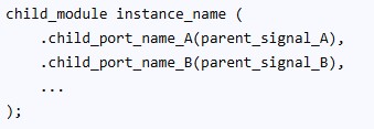
The top module used positional association in these instantiations. It follows the following rules: The parent signals are the signals in your top.
Therefore, in the example code, is adding the leading four zeros necessary? Is using 'thos' necessary?
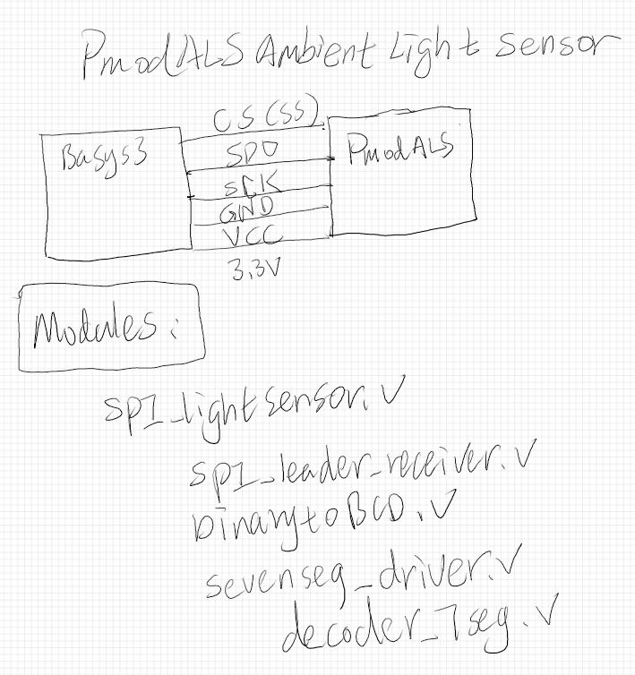
The PmodALS sensor is
plugged in to the top row of the JB pins on the Basys 3 baord.
Some changes must be made to the
constraint file to make it work. Make those changes to the contraint
file to make it work as demonstrated in the following video.
I used a flash light to test
the sensor. You can find that the maximum value is 255, which is the
8-bit binary value.
----------------------- Tasks: 1. Repeat the tasks in Section 2 (50 points) 2. A smart light controller: the goal is to detect the room brightness and control the LED light output. The
SPI transaction is periodically triggered to sample data from the Pmod
ALS. The sensor returns an 8-bit value representing the current light
level. PicoBlaze assembly code processes this 8-bit value and
determine how many LEDs to be turned on. The brighter the ambient
light, the less LEDs to be turned on. All LEDs should be on when it is
dimmer than a certain value.(100 points)