The Skyboard V2 lectures. Lecture 1 reads the schematic and board; Lecture 2 reviews the design and covers PCB design practice. Images are in the images folder next to this file.
Lecture 1: Reading the Skyboard
Lecture 1 · slide 1
CE351 · PCB DESIGN · LECTURE 1 OF 2
Reading the Skyboard
From schematic to copper: how an Arduino-Mega-class teaching board is built, block by block
mega.sch · mega.brd · Skyboard V2
Lecture 1 · slide 2
Big picture
System block diagram
USB-B
power + data
F1 PTC fuse
500 mA hold
+5 V rail
everything 5 V
LP2985 LDO
+3V3, 150 mA
ATmega16U2
USB ↔ UART bridge
ATmega2560
16 MHz · 256 KB flash
Peripherals
SD card via 74LVC125
Mic preamp → ADC0
PWM DAC → LM4862 → speaker
IR TX (0.5 A sink) + 38 kHz RX
RGB LED, buttons, LEDs
Mega headers, I²C, ultrasonic
Black = power flow · Blue = data (USB D±, UART, SPI, I²C, GPIO)
CE351 · PCB Lecture 1 · 02
Lecture 1 · slide 3
PART 1
Power & USB
Where the energy and the data come in: connector, protection, regulation and the USB-serial bridge.
Lecture 1 · slide 4
Power & USB
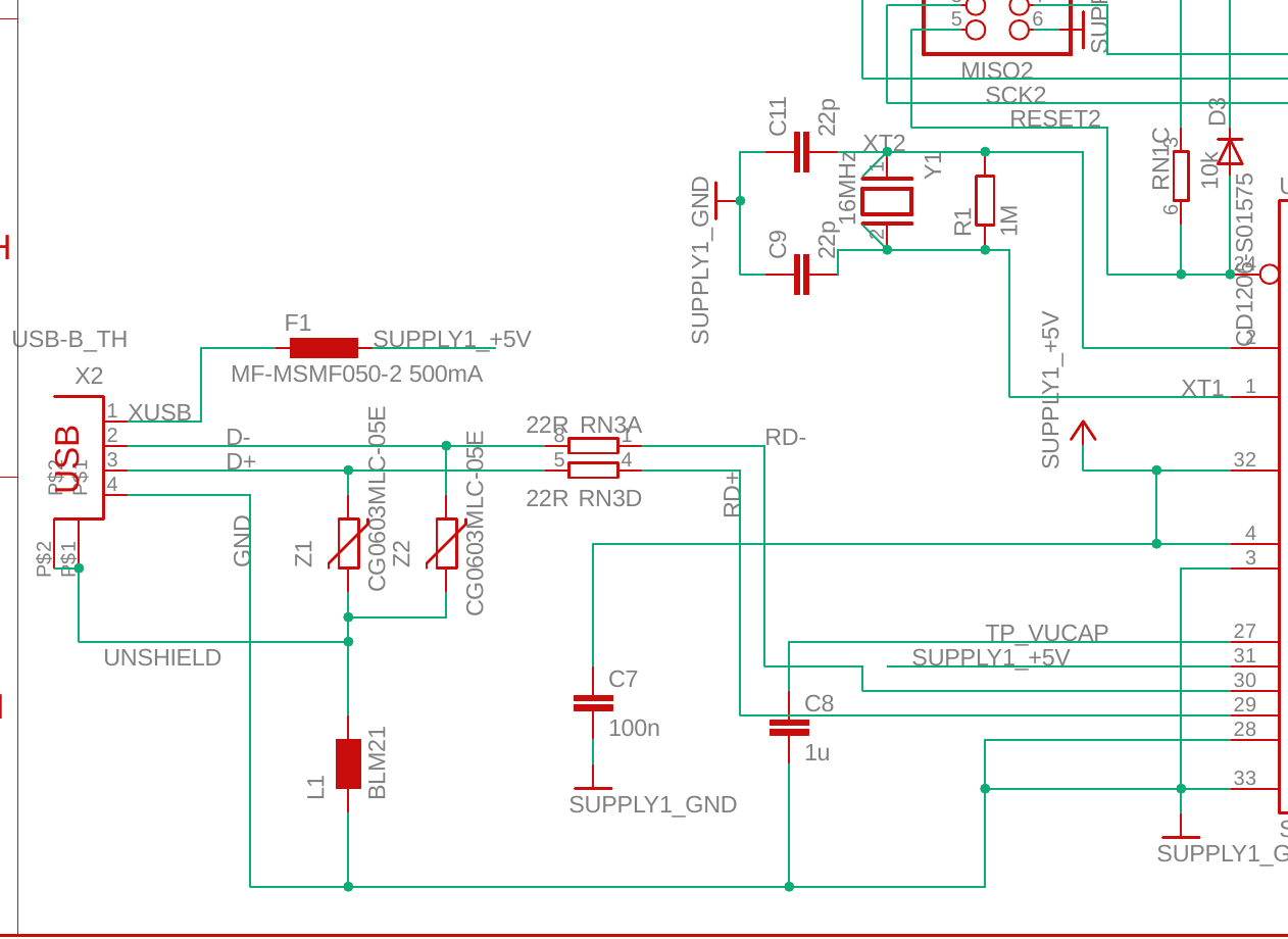
USB entry: fuse, ESD, terminations
F1 · MF-MSMF050
Resettable PTC: holds 500 mA, trips on a short, recovers when cooled.
Z1, Z2 · CG0603MLC-05E
Varistors clamp ESD on D− and D+.
L1 · BLM21 ferrite
Bonds the connector shield to GND through an HF impedance.
RN3 · 22 Ω
Series terminations on D± match the 16U2 driver to the ~90 Ω cable.
CE351 · PCB Lecture 1 · 04
Lecture 1 · slide 5
Power & USB
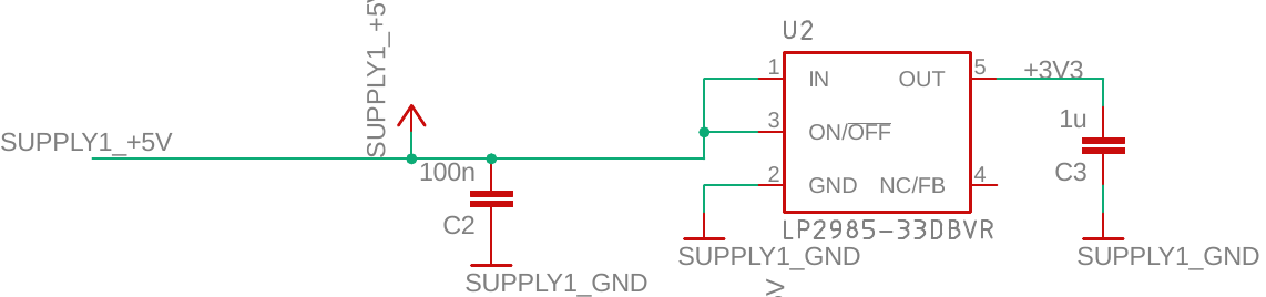
The 3.3 V island: LP2985-33
150 mA LDO
ON/OFF tied to IN: always on. Fixed 3.3 V output.
Loads
SD card, 74LVC125 buffer, 38 kHz IR receiver U1.
Heat check
P = (5 − 3.3) V × 0.1 A = 0.17 W at 100 mA — fine for SOT-23-5.
CE351 · PCB Lecture 1 · 05
Lecture 1 · slide 6
Power & USB
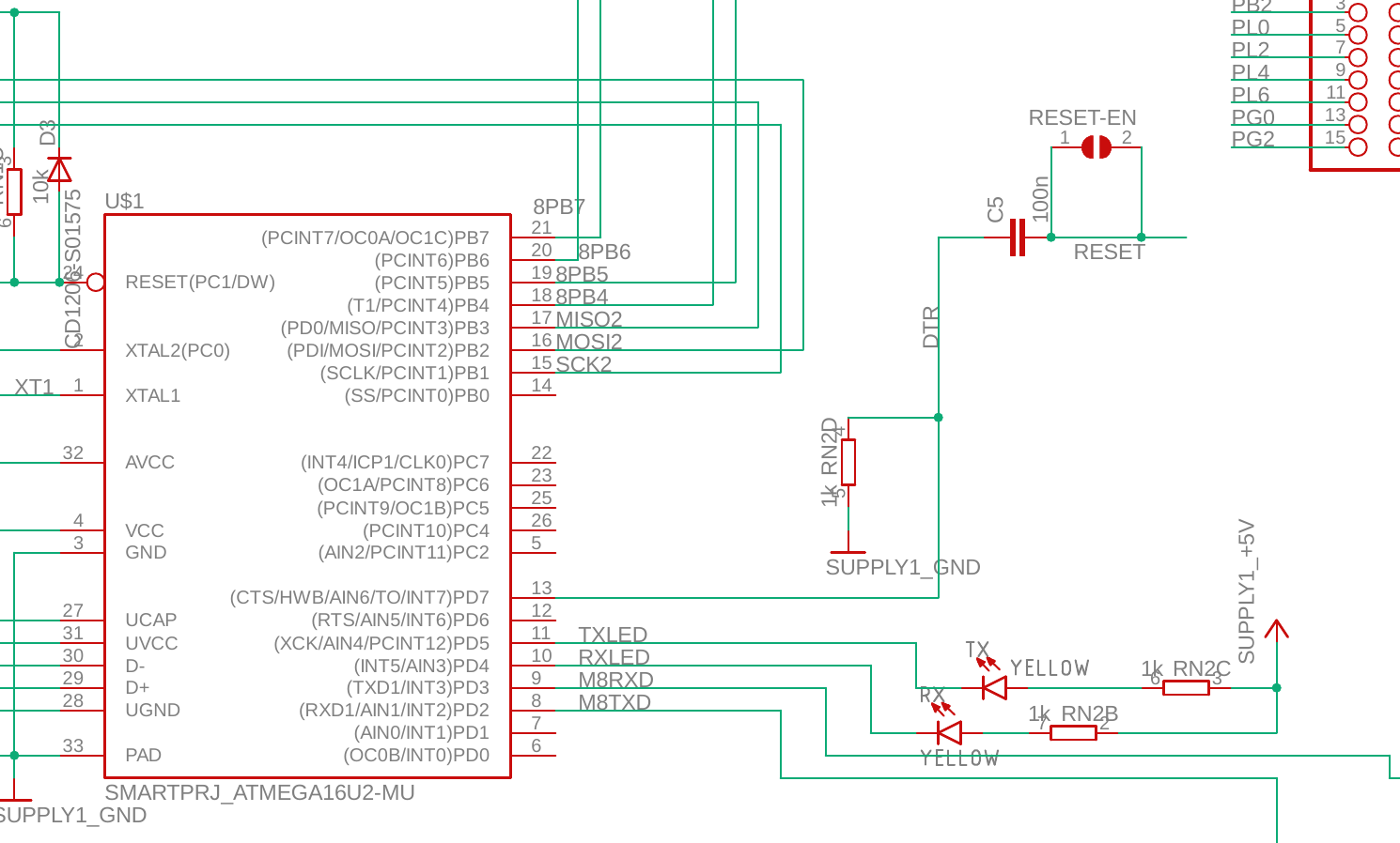
ATmega16U2: the USB-serial bridge
Auto-reset
DTR → C5 100 nF → RESET: a short pulse restarts the 2560 for upload.
RESET-EN
Solder jumper: cut it to stop resets when a terminal opens.
Serial link
M8TXD/M8RXD reach PE0/PE1 through 1 kΩ (RN6) — a header can override them safely.
ICSP1
6-pin header to reflash the 16U2 firmware.
CE351 · PCB Lecture 1 · 06
Lecture 1 · slide 7
PART 2
The main MCU
ATmega2560 core: supply pins, analog supply filter, clock, reset and how its pins reach the headers.
Lecture 1 · slide 8
Main MCU
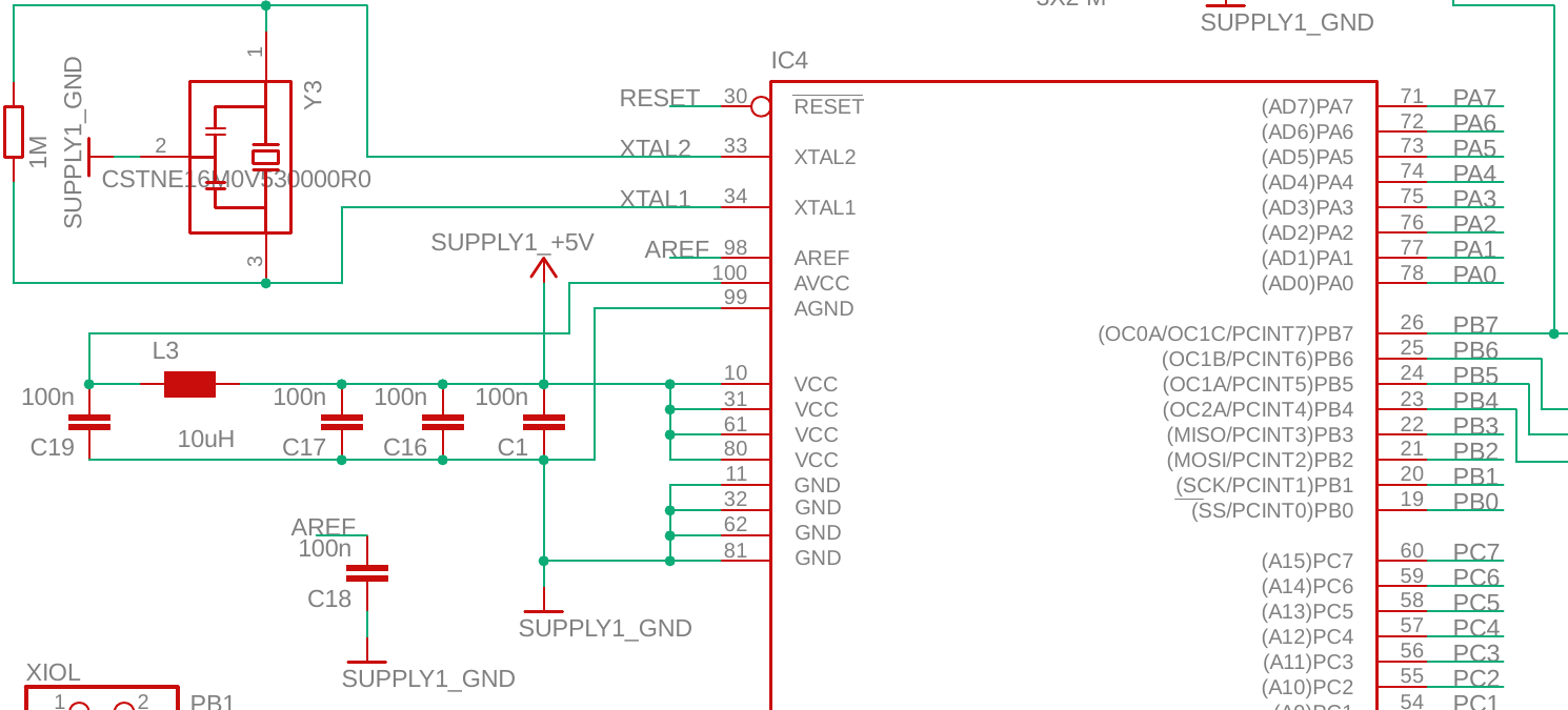
ATmega2560 core circuit
Decoupling
4 VCC/GND pairs; C1, C16, C17 = 100 nF. Where they sit matters (Lecture 2).
AVCC LC filter
L3 10 µH + C19 100 nF → f₀ = 1/(2π√LC) ≈ 159 kHz.
Clock
Y3 CSTNE16M0 resonator with built-in load caps; R23 1 MΩ.
Reset
10 kΩ pull-up, D5 clamp, ICSP2 and RESET2 button.
CE351 · PCB Lecture 1 · 08
Lecture 1 · slide 9
Main MCU
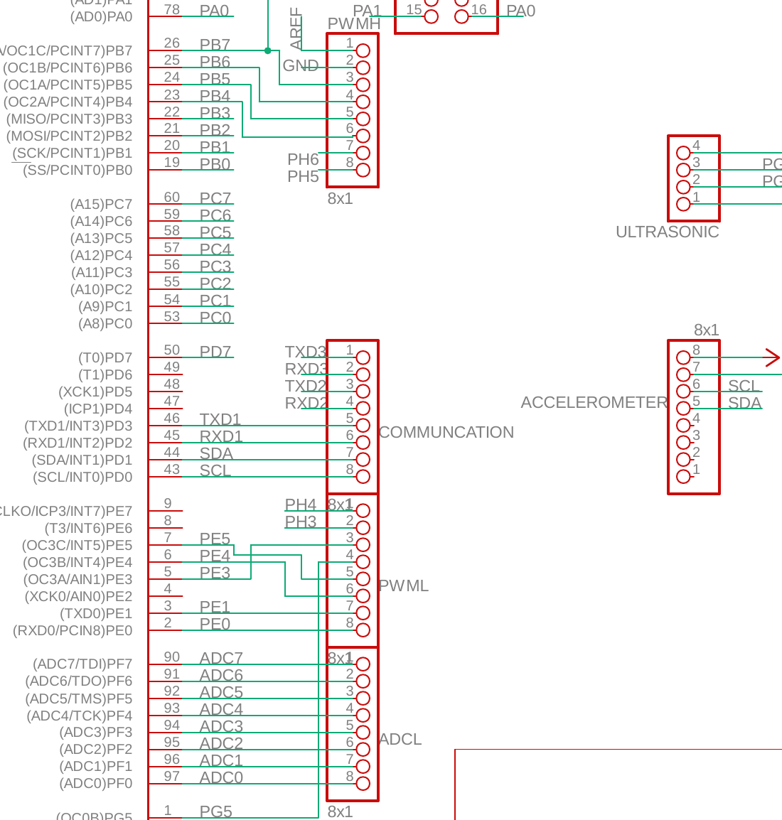
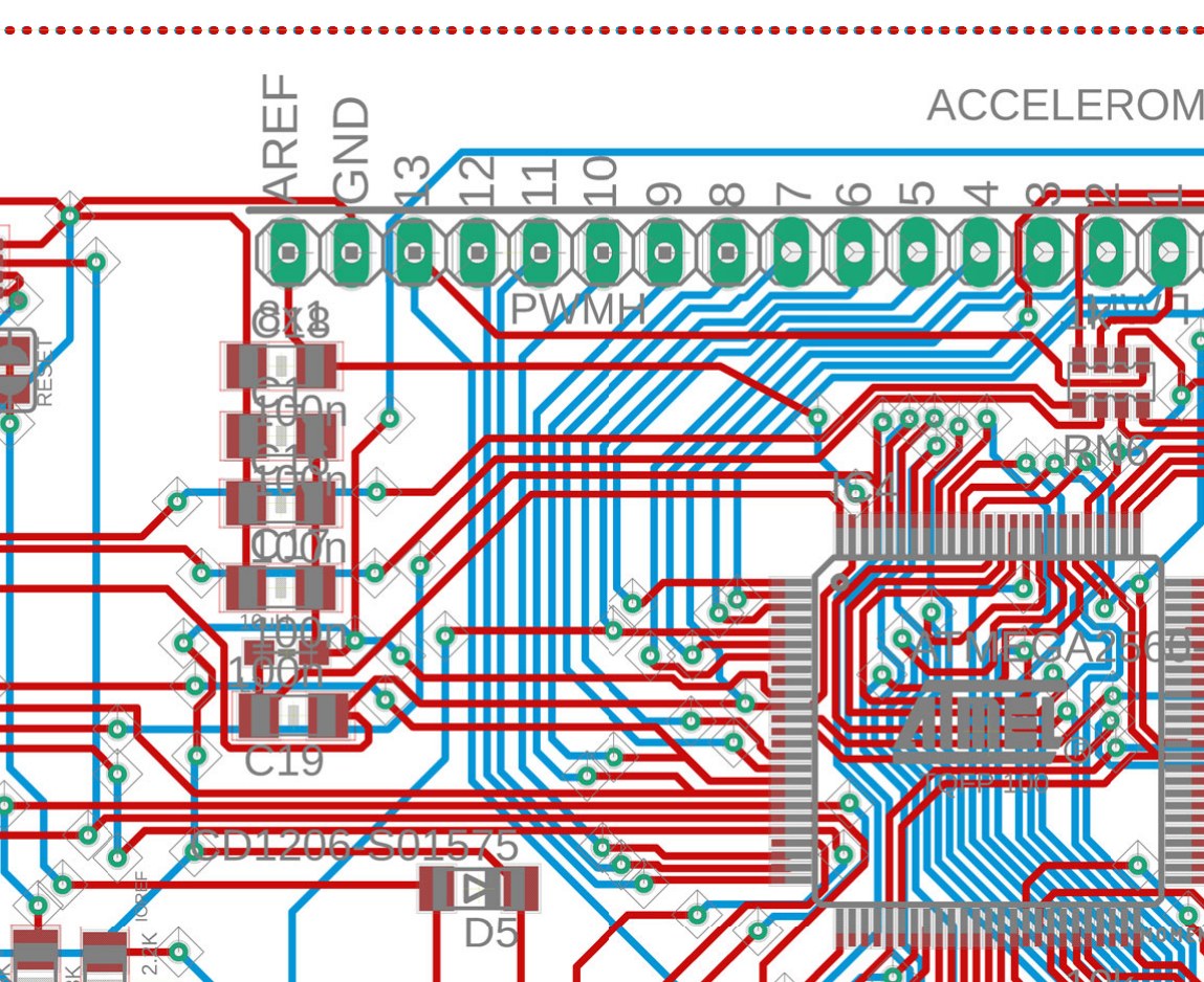
Arduino-Mega-compatible headers
Shield compatible
PWML/H, ADCL/H, COMMUNICATION and XIO follow Mega pin numbering.
Accelerometer
I²C (SDA/SCL) + 5 V, 10 kΩ pull-ups (RN5).
Ultrasonic
4-pin: 5 V, PG1, PG0, GND.
Watch for
Pins with two jobs — ADC0, PH5/PH6, the SPI pins.
CE351 · PCB Lecture 1 · 09
Lecture 1 · slide 10
PART 3
Peripherals
Storage, analog input, audio output and infrared — each with the numbers you can check from the schematic.
Lecture 1 · slide 11
Peripherals
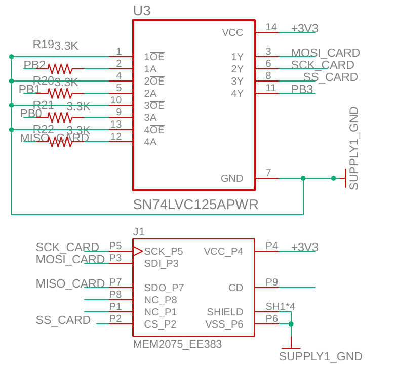
SD card: 5 V MCU, 3.3 V card
Down-shift
U3 runs at 3.3 V; LVC inputs tolerate 5 V, so PB0–PB2 → card is safe.
Series 3.3 kΩ
R19–R22 limit current into the buffer inputs.
Up-shift
Card MISO → 4A → 4Y → PB3: a 3.3 V high into a 5 V AVR.
Teaser
Look at the four OE pins. Are they all OK? (Lecture 2)
CE351 · PCB Lecture 1 · 11
Lecture 1 · slide 12
Peripherals
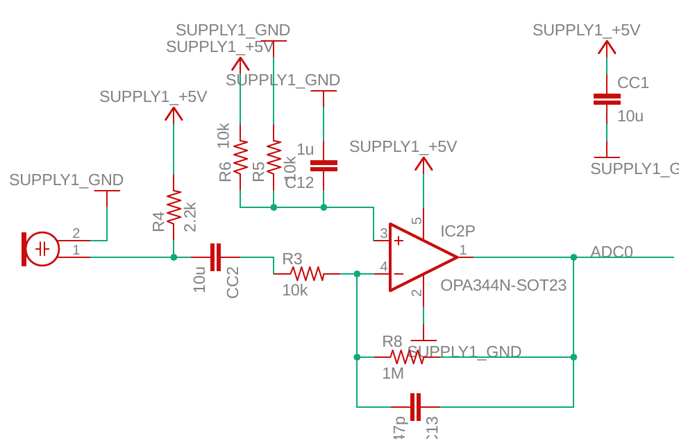
Microphone preamp: do the math
Quantity
From values
Bias point
R5 = R6 = 10 kΩ → 2.5 V
Gain
−R8/R3 = −1 M/10 k = −100 (40 dB)
Low corner
1/(2π·10 k·10 µ) ≈ 1.6 Hz
High corner
1/(2π·1 M·47 p) ≈ 3.4 kHz
Mic bias
R4 2.2 kΩ from +5 V
Output sits at 2.5 V — mid-scale for the 10-bit ADC — and swings ±2.5 V max.
CE351 · PCB Lecture 1 · 12
Lecture 1 · slide 13
Peripherals
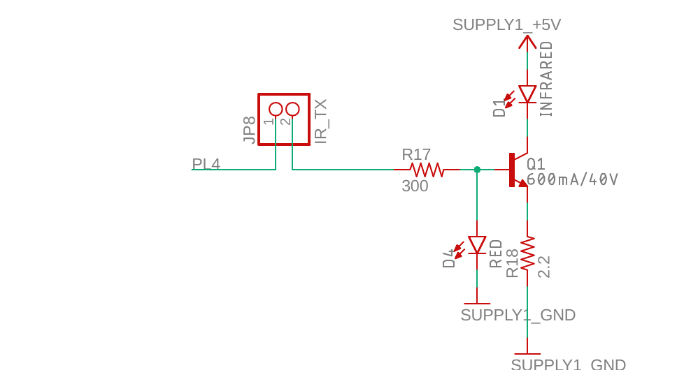
IR transmitter: an LED as a reference
Reference
Red LED D4 holds Q1’s base near 1.8 V.
Current sink
I ≈ (1.8 − 0.7) V / 2.2 Ω ≈ 0.5 A, nearly independent of the 5 V rail.
Base drive
(5 − 1.8) V / 300 Ω ≈ 11 mA from PL4 via JP8.
Receiver
U1 38 kHz demodulator on 3.3 V → PL5.
CE351 · PCB Lecture 1 · 13
Lecture 1 · slide 14
PCB 101
Anatomy of a two-layer board
Silkscreen — ink legend: ref-des, outlines
Solder mask — coating, open only at pads
Top copper — traces, pads (1 oz ≈ 35 µm)
FR-4 core — glass + epoxy, 1.6 mm typical
Plated via — drilled, then copper-lined
Bottom copper — second routing layer
Bottom mask; pads get a finish (gold)
Not to scale: the core is ~45× thicker than the copper. Gold strips = surface finish on exposed pads (HASL, ENIG or OSP).
CE351 · PCB Lecture 1 · 14
Lecture 1 · slide 15
PCB 101
From EAGLE layers to fab files
EAGLE layer
What it becomes
Typical Gerber file
1 Top
Top copper
.GTL
16 Bottom
Bottom copper
.GBL
17 Pads · 18 Vias · 44 Drills
Plated holes
Excellon drill (.XLN / .TXT)
29 tStop · 30 bStop
Solder-mask openings
.GTS / .GBS
21 tPlace · 25 tNames
Top silkscreen
.GTO
31 tCream
Paste stencil (assembly)
.GTP
20 Dimension
Board outline / routing
.GKO or .GM1
Mask layers are negative: what you draw on tStop is where the mask is removed. Always open the CAM output in a Gerber viewer before ordering.
CE351 · PCB Lecture 1 · 15
Lecture 1 · slide 16
PCB 101
Stackups and via types
2-layer (Skyboard)
Top · signals + parts
FR-4 core 1.6 mm
Bottom · signals / GND
4-layer
L1 · signals + parts
prepreg
L2 · solid GND
core
L3 · power pours
prepreg
L4 · signals
Through-hole via
Drilled through all layers. Cheapest; the only kind on Skyboard.
Blind via
Outer layer to an inner layer only. Extra process steps.
Buried via
Between inner layers; invisible from outside.
Microvia (HDI)
Laser-drilled, one layer deep. Phones and fine-pitch BGAs.
CE351 · PCB Lecture 1 · 16
Lecture 1 · slide 17
PCB 101
The building blocks of PCB wiring
Trace
The “wire”. Signals 0.2–0.25 mm wide; power wider (see Lecture 2).
Clearance
Copper-to-copper gap. Low-cost fabs: about 0.15 mm (6 mil) minimum.
Via
Plated hole that changes layer, e.g. 0.3 mm drill in a 0.6 mm pad.
Pad & footprint
Copper land pattern for a part, from its datasheet or IPC-7351.
Pour / plane
Large copper area on one net, usually GND, joined to pads by thermal spokes.
Keep-out
No copper or parts allowed: board edge, mounting holes, antennas.
CE351 · PCB Lecture 1 · 17
Lecture 1 · slide 18
PCB 101
Routing tricks that save a respin
Avoid: acute angle (acid trap)
Prefer: 45° bends
Place before you route
Placement decides most of the routing quality.
Critical nets first
Power, clocks, USB and analog; wide buses last.
One direction per layer
On 2 layers: top mostly horizontal, bottom vertical, via at each turn.
Fan out big ICs
Short stubs and vias outward from QFP pins before routing buses.
Net classes + DRC
Width and clearance per class; let the DRC police them.
Short and direct
Few vias, no stubs or loops; enter pads straight, not at a slant.
CE351 · PCB Lecture 1 · 18
Lecture 1 · slide 19
PART 4
From schematic to copper
How the netlist became a two-layer board: layers, placement and floor plan.
Lecture 1 · slide 20
Layout
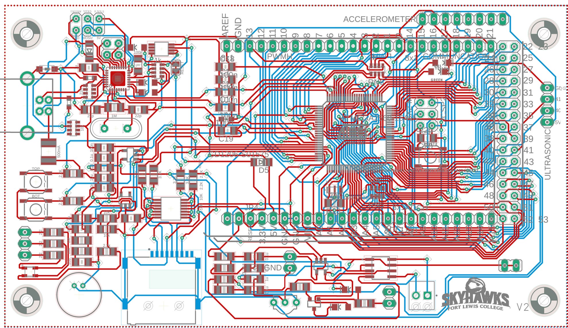
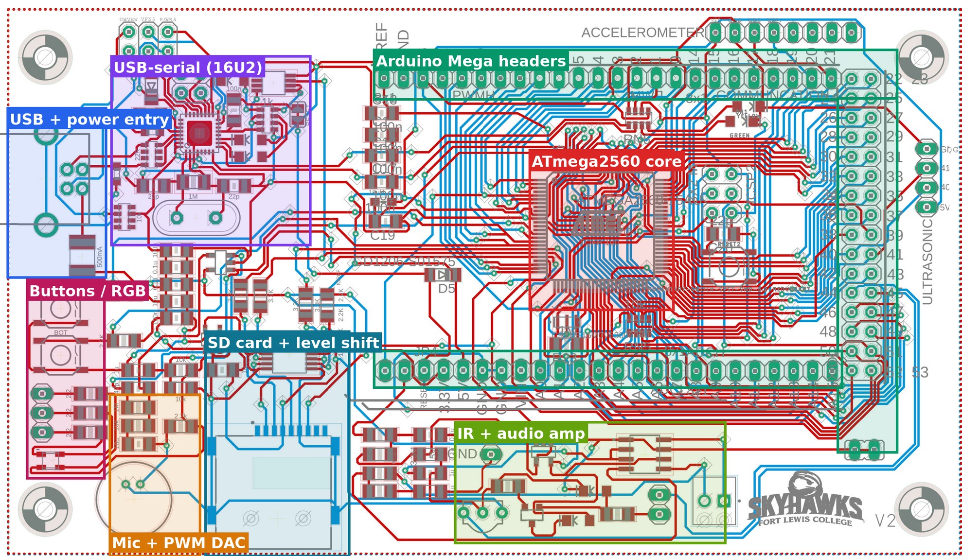
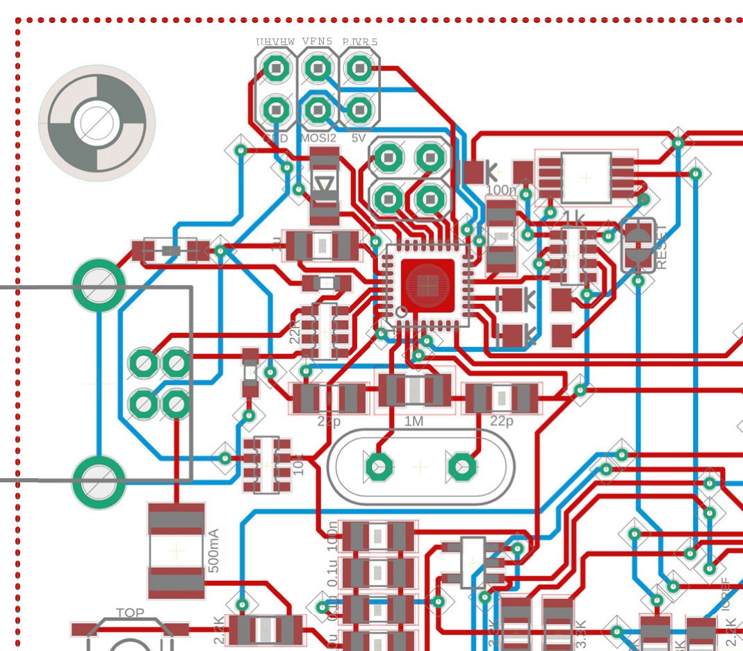
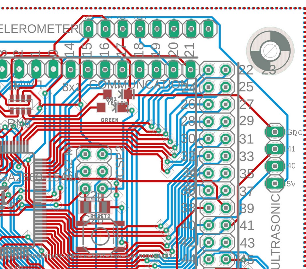
Reading the layout plot
Red / blue
Top / bottom copper. Two layers, no internal planes.
Green rings
Through-hole pads and vias.
Grey
Silkscreen, outlines, part values.
Corners
Four 2.8 mm mounting holes, Arduino-style header rows.
CE351 · PCB Lecture 1 · 20
Lecture 1 · slide 21
Layout
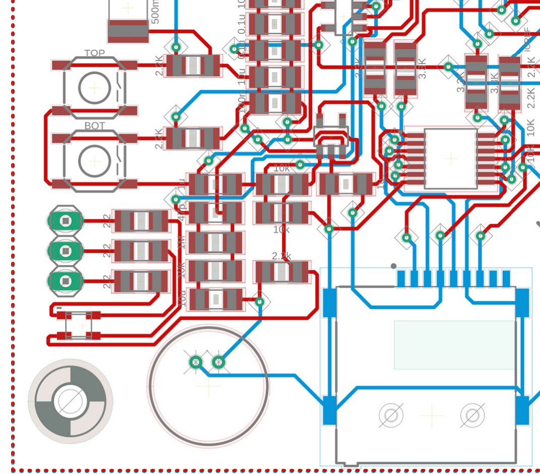
The floor plan
Edges first
Connectors (USB, SD, headers) are placed by mechanics.
MCU centre
The 2560 sits where its 86 I/O fan out to all headers.
Analog corner
Mic and PWM DAC grouped bottom-left.
Question
Does each zone have a quiet return path? (Lecture 2)
CE351 · PCB Lecture 1 · 21
Lecture 2: Design review and PCB tricks
Lecture 2 · slide 1
CE351 · PCB DESIGN · LECTURE 2 OF 2
Design review & PCB tricks
What we would change on Skyboard V2 — and the habits that prevent these problems on your next board
Lecture 2 · slide 2
Method
How to run a design review
Must fix
Can damage parts, break a function or exceed a rating.
Should fix
Works today but with thin margin: noise, timing, heat.
Verify
Looks wrong — confirm against the datasheet or the intent.
Nice to have
Manufacturing, test and documentation polish.
Order of work: schematic (ratings, interfaces, unused pins) → layout (returns, decoupling, sensitive nets) → DFM (silk, assembly, test). Write each finding as observation → risk → fix.
CE351 · PCB Lecture 2 · 02
Lecture 2 · slide 3
Skyboard V2
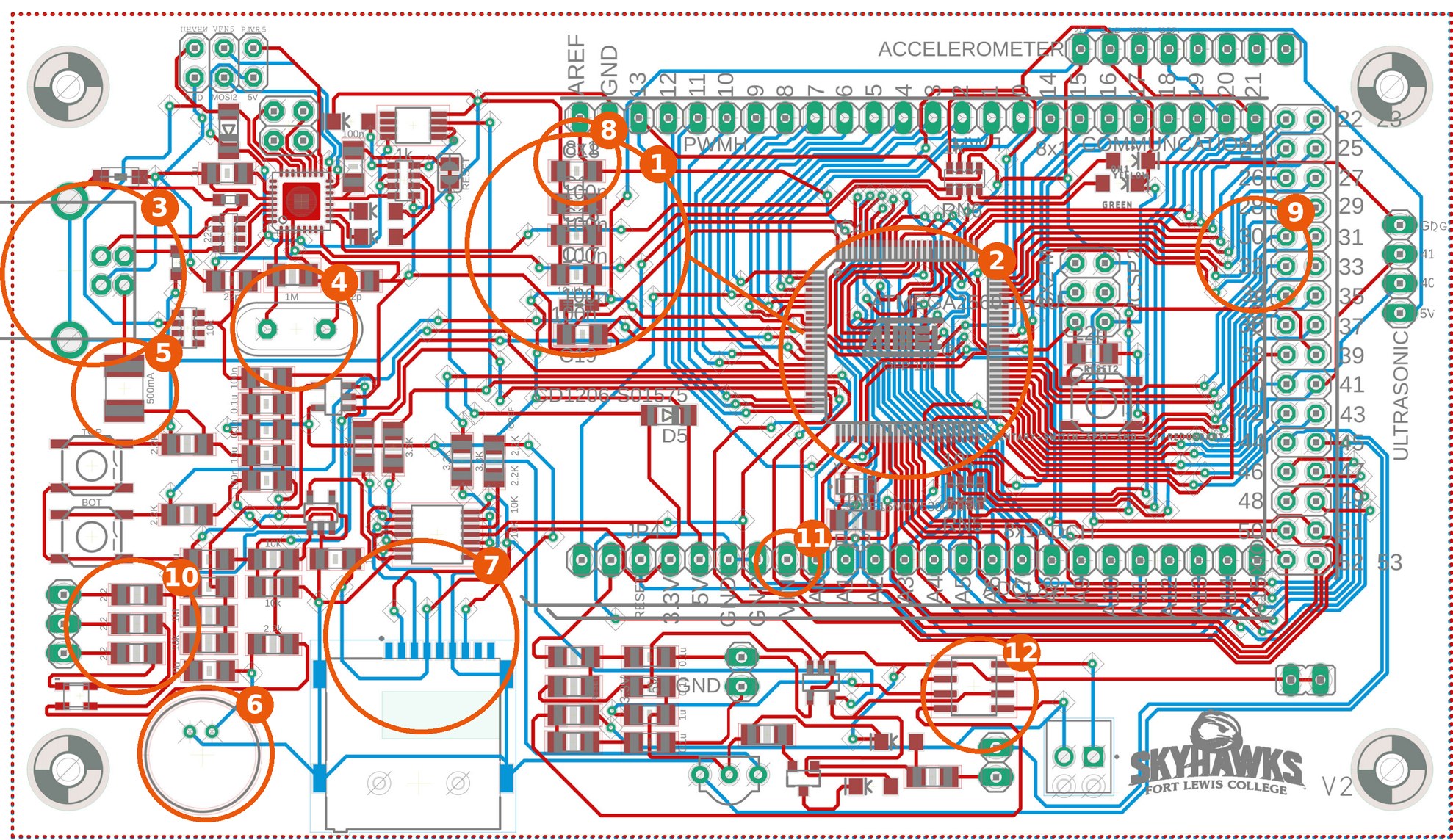
Finding map
01 Decaps ~20 mm from MCU
02 No local decoupling / no GND plane
03 USB pair & ESD placement
04 16U2 crystal (HC-49) distance
05 Thin 5 V path from F1
06 Mic beside digital lines
07 SD socket + LVC125 area
08 Silkscreen overlaps (C18/C19)
09 Header labels over pads
10 RGB LED 2.2 Ω resistors
11 VIN pin not connected
12 Audio amp & speaker
CE351 · PCB Lecture 2 · 03
Lecture 2 · slide 4
PART 1
Schematic findings
Ratings, interfaces and unused pins — problems you can catch before any copper exists.
Lecture 2 · slide 5
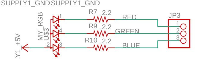
Finding 10
RGB LED resistors: 2.2 Ω
MUST FIX
Demand
(5 − 2.0 − 0.3) V / 2.2 Ω ≈ 1.2 A on the red channel.
Limit
An ATmega pin is rated 40 mA absolute max; the LED itself ~20–30 mA.
Fix
Red ≈ 330 Ω, green/blue ≈ 220 Ω → ~9 mA each. Or confirm 2.2 kΩ was meant.
CE351 · PCB Lecture 2 · 05
Lecture 2 · slide 6
Finding (IR TX)
IR driver: power at 0.5 A
MUST FIX
Q1 if PL4 stays high
V꜀ₑ ≈ 5 − 1.5 − 1.1 = 2.4 V → ≈1.2 W vs ~0.35 W for SOT-23.
R18
I²R = 0.5² × 2.2 = 0.55 W vs 0.125–0.25 W for a chip resistor.
Budget
0.5 A ≈ the entire USB budget; pulses droop the shared 5 V.
Fix
Cap duty in firmware + higher-power R18 and SOT-89/MOSFET, or ~100–200 mA. Add a 100–470 µF reservoir.
CE351 · PCB Lecture 2 · 06
Lecture 2 · slide 7
Finding (SD bus)
74LVC125: MISO buffer always on
MUST FIX
Observation
4OE is tied to GND, so 4Y drives PB3 (MISO) all the time.
Risk
During ISP the 2560 drives MISO too → contention. No other SPI device can share the bus.
Fix
Drive 4OE from SS_CARD so it only talks when the card is selected.
Also
Add a 10 kΩ pull-up on SS so the card stays deselected during reset.
CE351 · PCB Lecture 2 · 07
Lecture 2 · slide 8
Finding (interfaces)
3.3 V signals into a 5 V AVR
SHOULD FIX
0.3 V
margin: 3.3 V high vs V_IH(min) = 0.6 × 5 V = 3.0 V
Signal
Path
Better option
MISO
card → 4Y → PB3
74HCT125 at 5 V (VIH 2.0 V)
IR RX
U1 out → PL5
Open-collector + pull-up to 5 V
Any
3V3 → 5V
74LVC1T45 dual-supply translator
CE351 · PCB Lecture 2 · 08
Lecture 2 · slide 9
Finding (LDO)
3.3 V rail: output cap and decoupling
VERIFY
C3 = 1 µF
LDO stability depends on output C and ESR. Check the LP2985 minimum — likely 2.2 µF.
SD inrush
Cards pull current spikes at insertion and writes: add 10 µF at J1.
U3 decoupling
No 100 nF shown at the 74LVC125 VCC pin: add one.
CE351 · PCB Lecture 2 · 09
Lecture 2 · slide 10
Finding (op-amp)
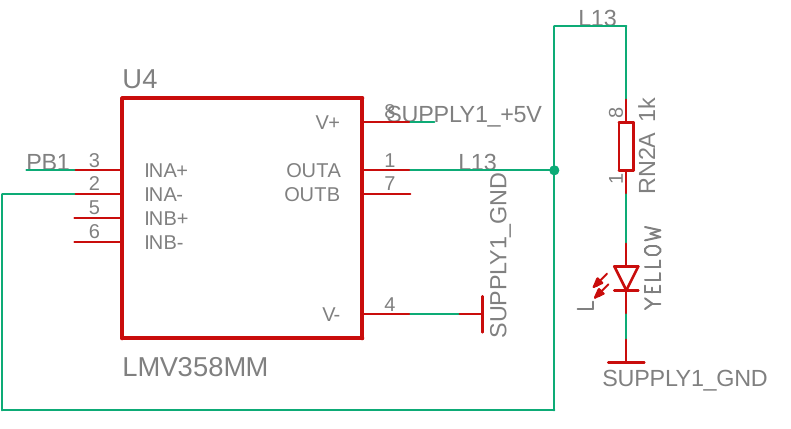
LMV358: floating second half
SHOULD FIX
Observation
INB+ and INB− are unconnected; OUTB is open.
Risk
Floating inputs can oscillate, add supply current and inject noise.
Fix
Wire B as a follower: OUTB → INB−, INB+ to a fixed voltage (GND or mid-rail).
Verify
L13 is driven from PB1 (SCK), not PB7. Intentional SPI activity LED?
CE351 · PCB Lecture 2 · 10
Lecture 2 · slide 11
Finding (pin map)
Pins with two jobs
SHOULD FIX
Pin
Also connected to
Risk
Fix
ADC0
Mic preamp output + ADCL header
A user sensor fights the op-amp
Jumper or 1 kΩ series
PH5, PH6
2.2 kΩ pull-ups + buttons; PWMH D8/D9
PWM loaded, inputs read high
Jumper; document
PB1–PB3
LVC125, L13 buffer, ICSP2
Bus contention (see SD)
OE control
SDA, SCL
10 kΩ pull-ups to 5 V
Overstress on 3.3 V-only modules
Pull-ups on module side
CE351 · PCB Lecture 2 · 11
Lecture 2 · slide 12
Finding (supply & ESD)
Quiet supplies and real ESD paths
SHOULD FIX
ESD return
Z1/Z2 clamp to the shield node, which reaches GND only via L1. A ferrite slows the very edge you want to shunt.
Fix
TVS array (e.g. USBLC6-2) at the connector, GND via right at its pin.
Mic bias
R4 feeds the mic from raw 5 V: add RC, e.g. 1 kΩ + 10 µF (f꜀ ≈ 16 Hz).
VIN
Header VIN connects to nothing: mark N/C or remove.
CE351 · PCB Lecture 2 · 12
Lecture 2 · slide 13
PART 2
Layout findings
Return paths, decoupling, sensitive nets and manufacturability.
Lecture 2 · slide 14
Finding 2
No ground plane: where does current return?
SHOULD FIX
V2 · return via thin traces
Big loop area (shaded) → inductance, ground bounce, EMI.
V3 · solid GND pour
High-frequency return hugs the trace in the plane beneath.
CE351 · PCB Lecture 2 · 14
Lecture 2 · slide 15
Finding 1
Decoupling caps ~20 mm from the MCU
MUST FIX
Observation
C1/C16/C17/C19 sit together, ~20 mm (measured on plot) from the VCC pins.
Why it matters
~1 nH/mm → ~20 nH. V = L·di/dt = 20 nH × 50 mA / 2 ns ≈ 0.5 V spike.
Fix
One 100 nF per VCC/GND pair, ≤3 mm, on the IC’s side; vias straight to GND.
Keep
C19 at AVCC (pin 100) and C18 at AREF (98), as close as possible.
CE351 · PCB Lecture 2 · 15
Lecture 2 · slide 16
Findings 3 & 4
USB pair and crystal placement
SHOULD FIX
USB D±
Route as a tight coupled pair (~90 Ω differential), no layer swaps, over unbroken GND.
ESD
Put the protector within a few mm of the connector, before anything else.
Crystal
HC-49 sits below the caps; use a 3.2 × 2.5 mm SMD part beside XTAL1/2.
Keep-out
No other signals under the crystal; GND under and around it.
CE351 · PCB Lecture 2 · 16
Lecture 2 · slide 17
Finding 5
Power traces: heat vs. voltage drop
SHOULD FIX
IPC-2221 external trace, 1 oz Cu, 10 °C rise: I = 0.048·ΔT^0.44·A^0.725
Current
Min width (heat)
0.5 A
≈ 0.11 mm (4.5 mil)
1 A
≈ 0.30 mm (12 mil)
2 A
≈ 0.78 mm (31 mil)
3 A
≈ 1.37 mm (54 mil)
Drop is the real limit
1 oz ≈ 0.5 mΩ/□. A 0.25 mm × 100 mm trace = 400 □ ≈ 0.2 Ω → 0.1 V lost at 0.5 A.
V3 rule
5 V from F1: ≥ 0.6–1.0 mm or a pour. Signals stay 0.2–0.25 mm.
CE351 · PCB Lecture 2 · 17
Lecture 2 · slide 18
Finding 6
Microphone next to digital lines
SHOULD FIX
Observation
Mic and its gain-of-100 preamp sit beside SD SPI traces and the button/RGB area.
Risk
Coupled clock edges are amplified 100× into ADC0.
Fix
Op-amp right at the mic; short input trace; GND pour around; SPI routed away.
Partition
Analog corner over unbroken GND — one plane, separated by placement, not cuts.
CE351 · PCB Lecture 2 · 18
Lecture 2 · slide 19
Findings 8 & 9
Silkscreen and manufacturability
NICE TO HAVE
Silk
Overlapping refdes (C18/C19), text across pads and vias, long values printed (CD1206-S01575).
Assembly
SD socket pads are on the bottom layer — confirm side; two-sided assembly costs more.
Test
Only TP_VUCAP: add 5V, 3V3, GND test points and loops.
Fab
Add 3 fiducials if the board will be machine-assembled.
CE351 · PCB Lecture 2 · 19
Lecture 2 · slide 20
Summary
V3 change list
#
Change
Severity
Effort
1
RGB resistors 220–330 Ω
Must
BOM only
2
IR driver: power parts + duty limit
Must
Parts + firmware
3
4OE ← SS_CARD; SS pull-up
Must
Reroute
4
Decaps at every VCC pin
Must
Placement
5
Bottom GND pour + stitching
Should
Re-route
6
5 V-level MISO / IR RX
Should
1 part
7
LDO C3 ≥ datasheet min; 10 µF at SD
Verify
BOM
8
Tie off LMV358 B; mic bias RC
Should
2–3 parts
9
TVS at USB; SMD crystal
Should
Placement
10
Silk, test points, fiducials
Nice
Cosmetic
CE351 · PCB Lecture 2 · 20
Lecture 2 · slide 21
PART 3
PCB design tricks
General habits that would have caught most of today’s findings — on any board, in any tool.
Lecture 2 · slide 22
Trick 1
Choose the stackup first
Layer
2-layer (V2)
4-layer option
L1
Signals + parts
Signals + parts
L2
Signals + GND
Solid GND
L3
—
Power (5 V / 3V3 pours)
L4
—
Signals
For a dense QFP-100 board, 4 layers buys a solid reference plane, short decoupling loops and easier routing. At prototype fabs the price gap is now small — compare quotes before deciding.
CE351 · PCB Lecture 2 · 22
Lecture 2 · slide 23
Trick 2
Ground plane rules
Don’t cut it
Never route a slot under a fast signal: its return must detour around.
Stitch it
Vias tying top and bottom GND along edges and near every layer change.
Keep it whole
Bottom traces short and perpendicular, so the pour stays connected.
One ground
Partition analog/digital by placement; avoid split planes.
CE351 · PCB Lecture 2 · 23
Lecture 2 · slide 24
Trick 3
Decoupling recipe
Values
100 nF per power pin + 1–10 µF bulk per rail per IC cluster.
Distance
≤ 3 mm, same side as the IC, small package (0402/0603).
Order
Rail → cap pad → IC pin; the cap sits in the current path.
Vias
Short, wide via from the cap’s GND pad straight to the plane; don’t share.
Place decaps before routing anything else around a big IC — they own the space next to the pins.
CE351 · PCB Lecture 2 · 24
Lecture 2 · slide 25
Trick 4
Vias, heat and thermal relief
Power vias
Use several in parallel for power; a single small via is a bottleneck.
Thermal vias
Array under exposed pads (16U2 PAD, regulators) into a GND pour.
Thermal relief
Spokes on pour connections for TH pads so they can be soldered.
Teardrops
Fillets where traces meet pads/vias resist cracking and drill drift.
CE351 · PCB Lecture 2 · 25
Lecture 2 · slide 26
Trick 5
Sensitive and fast nets
Net type
Rule of thumb
Differential (USB, Ethernet)
Coupled pair, set impedance, match length, no stubs or layer swaps
Crystals / resonators
Within a few mm of the pins, GND under, nothing else under
Clocks, SPI SCK
Short, over plane, 3W spacing from neighbours
High-Z analog (mic, sensors)
Shortest path, guard with GND, away from clocks
Switching power
Tiny hot loop; input cap right at the switch
CE351 · PCB Lecture 2 · 26
Lecture 2 · slide 27
Trick 6
Design for manufacture
Fab rules first
Load the fab’s DRU (e.g. 6/6 mil, annular ring) before routing.
No acid traps
Avoid acute trace angles; use 45° bends.
Mask slivers
Keep mask webs between fine-pitch pads above the fab minimum.
Assembly
Single-sided SMD if possible, fiducials, consistent footprints, pin-1 marks.
Test
Test points on every rail and key bus; label them.
Check outputs
Review Gerbers in a viewer, not just the CAD view.
CE351 · PCB Lecture 2 · 27
Lecture 2 · slide 28
Trick 7
Silkscreen that helps
Readable
Refdes 0.8–1.0 mm tall, 0.15 mm stroke; hide values.
Never on pads
Silk is clipped by the mask opening — move it.
Polarity
Pin-1 dots, diode bars, + marks visible after assembly.
Board ID
Name, rev, date, and a short QR to the docs repo.
CE351 · PCB Lecture 2 · 28
Lecture 2 · slide 29
Take-home
Your review checklist
Schematic
Layout
Every part within its ratings (I, P, V)
Decaps at every pin, before routing
Voltage domains: VIH/VOL margins
Continuous return plane under fast nets
Unused pins and gates tied off
Power traces sized for drop
Shared pins documented / jumpered
Sensitive nets short and guarded
ESD at every connector
Silk off pads; test points; fiducials
CE351 · PCB Lecture 2 · 29
Lecture 2 · slide 30
ASSIGNMENT
Ship Skyboard V3 on paper.
Pick three items from the change list and implement them in EAGLE.
Show the math for each: current, power, margin or loop size.