If you’ve never had a board manufactured, then hearing about Gerbers, Excellon, and NC Drill Files might sound like a foreign language.
Instead of relying on native file formats, every PCB design tool supports an intermediary manufacturing files, called Gerbers. These files describe the copper of every layer in your PCB in a way that a computer-aided manufacturing system (CAM) can understand. When Gerber artwork was first invented, they were used to provide instructions to a photoplotter machine that would create a picture of your PCB using light on a unexposed piece of film. These days, Gerbers are used to controls a laser plotting machine to make an image of all the traces, holes, vias on your PCB layout.
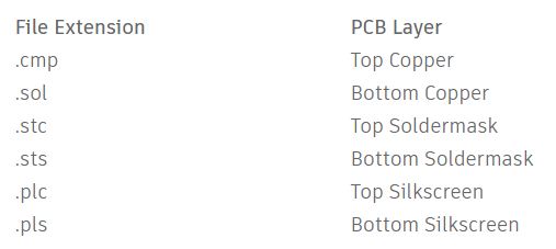
The trick with Gerbers is that every file you generate will be associated with a particular layer on your board layout, each with its own unique file extension. The standard file extensions you’ll work within Autodesk EAGLE today include:
Another thing to remember about Gerbers is their available formats – Gerber RS-274D and Gerber RS-274X. The D format is the older standard and will use two files per layer on your PCB. The newer X standard has done away with the two file format and contains all of the information about a layer in a single file. Regarding having to manage your design data, this makes it a whole lot easier when you only have to keep track of one file per layer instead of two. We’d always recommend using the Gerber RS-274X format; there’s no reason not to these days.
How About Those Drill Holes? (Drill holes are not through-holes or pads for soldering. Drill holes are for screws to mount your board somewhere).
You might have noticed that one thing missing from the table above is any reference to a drill file. This is actually as a secondary file that you’ll need to send to your manufacturer along with your Gerbers. The NC (Numeric Controlled) Drill File will be used to determine exactly where all of your drill holes are placed on your board and what size they need to be. Just as a heads up, you might also hear of an NC Drill File being referred to as an Excellon file, which is based on the drilling and routing machines that were made by the Excellon corporation back in the day. Now that you’ve got a general idea of what Gerber and Drill Files are about let’s dive into Autodesk EAGLE and see how to generate them.
Generating Your Gerber Files
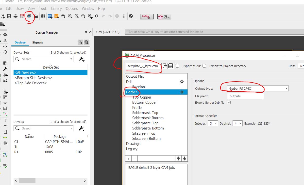
Autodesk EAGLE includes a handy computer-aided manufacturing (CAM) processor that allows you to load a CAM file and quickly generate the specific files you need for your design. In our example, we’re going to load up the Gerber RS-274X CAM file.
-Open your PCB layout (.brd) file in the Autodesk EAGLE Control Panel.
-Next, select the CAM Processor cam-icon tool at the top of your interface or select File » CAM Processor to open the CAM Processor dialog.
It is a two-step process, the first one is to create all the gerber files, the second step is to create the drill file. But in the newer version of Eagle PCB, all the gerber files including the drill file will be generated at the same time after you go through the following process.
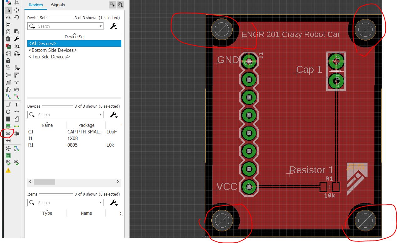
Before we can create the drill file, we need the drill-holes at the four corners of the board. Change the diameter to 3 mm.
When you are ready, just run the CAM processor and all your files will be ready in your local drive.
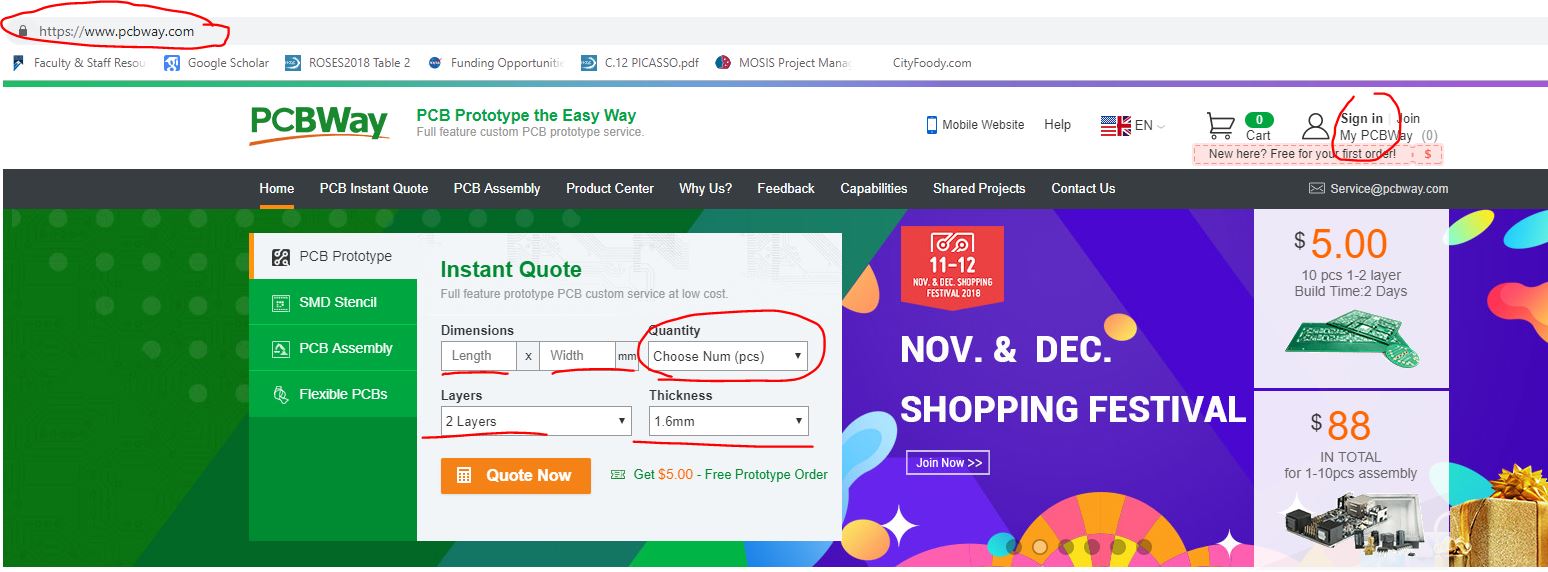
There are many PCB manufacturers. I have been working with PCBway for a while and I found this company can do really fair jobs with a low cost. Go ahead and register for an account. After you upload your gerber files, they will have their PCB engineers to check if you have a complete list of required files for the run. This check just takes less than 24 hours even though it is during the weekend (based on my experience, don't blame me if they can't do it now).
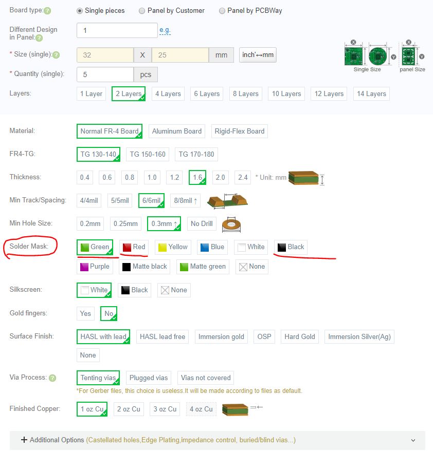
Measure the dimension of the board and type it in the quote window, choose the quantity to be 5 pieces, 2 layers, and keep the default thickness.
You can customize these following properties of your board. It is fine to keep the default ones, which is the cheapest one. Other options may change the cost a little bit.
You can change the color of the soldermask to be RED or BLACK. The GREEN one is the most common color though.
Finally, when you are ready, put all the gerber files into one .zip file and upload it in PCBway's portal. They will send you an email if there is nothing wrong with the design. After you checked it out, they will be able to fabricate it and send it to the US in 1-2 weeks.
If you want me to pay this fabrication for you using my research fund, come to my office to show your PCB and your approved gerbers in PCBway, I'll let you know if I will order this for you.
I'll be very glad to pay your PCB if it is a good work. It will be even more amazing if you can use SMT components for your design. You design may become an educational kit for local high school students. If you are interested, we can develop more things like this and organize these kits in a website as your Senior Seminar project in the future, if possible !! Exciting !!!
The address is:
Yiyan Li
1000 Rim Dr.
Department of Physics & Engineering
Durango, CO 81301