Tutorial
6: Placing circuit layouts
Begin
by copying the library, Tutorial_5, into a new library called
Tutorial_6.Ensure, when you copy, that “update instances” is selected
so that the new library doesn’t reference cells in the other libraries.
Create a new layout cell called "pad"
If we have 12 pad cells on a side (10 plus two corners) then each cell
must be 1.5mm/12 or 125 um.
In order to ensure this pad falls on the 0.15 um grid let’s reduce the
pad cell size to 120 um.
This also ensures that the final chip size is smaller than the 1.5 mm
square size we are allowed.
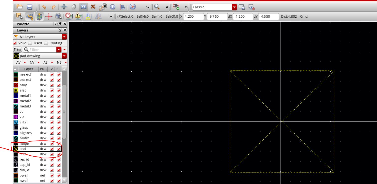
Select the pad layer and add an arbitrary size rectangle as seen below.
The pad layer has no fabrication significance (so you really don’t need
it).
We’ll use the pad layer as an outline for the cell. We could also use
the text layer for a cell outline.
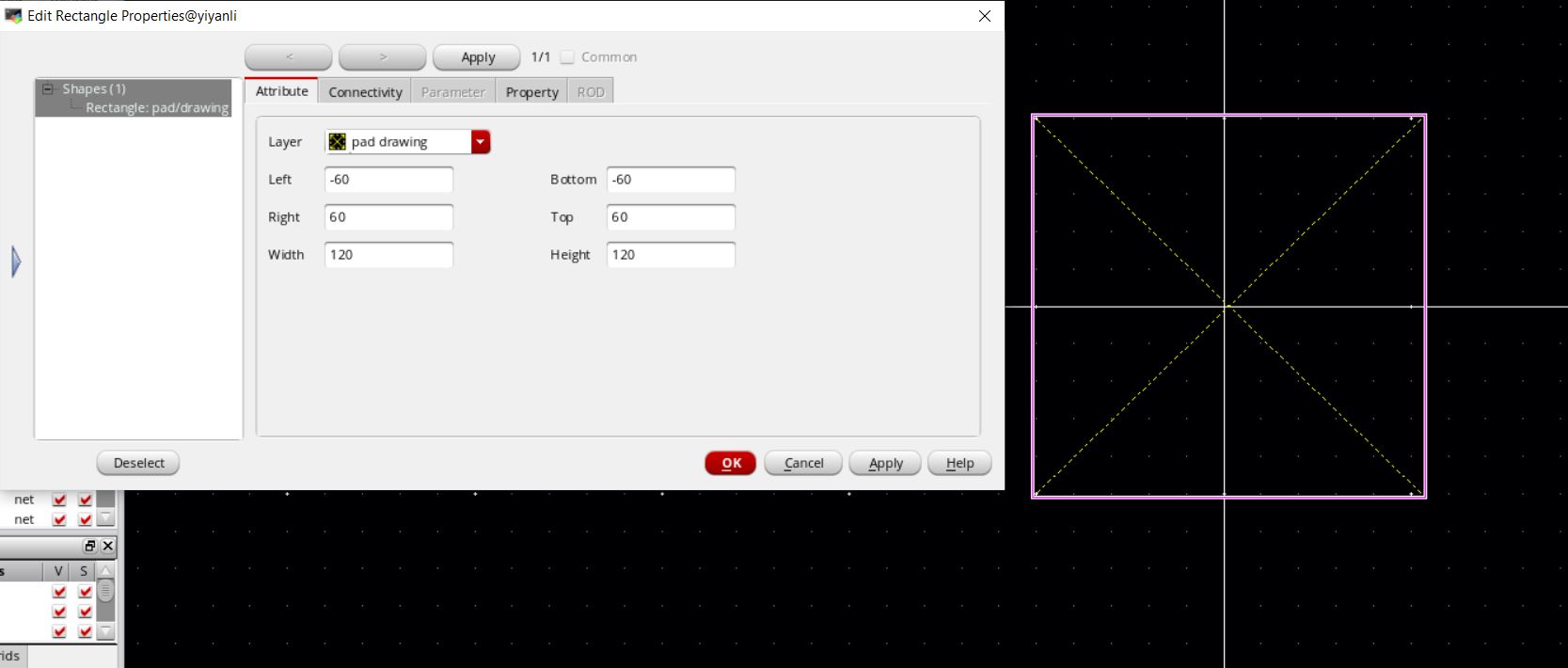
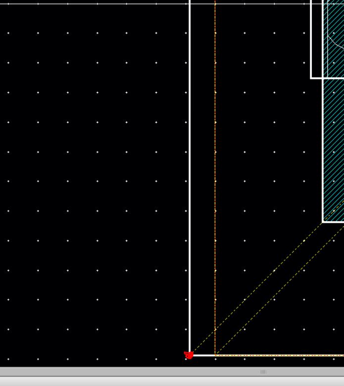
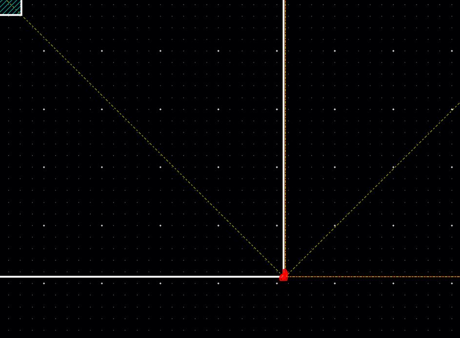
Next edit the rectangle’s properties so that it is 120 um square
centered upon the origin.
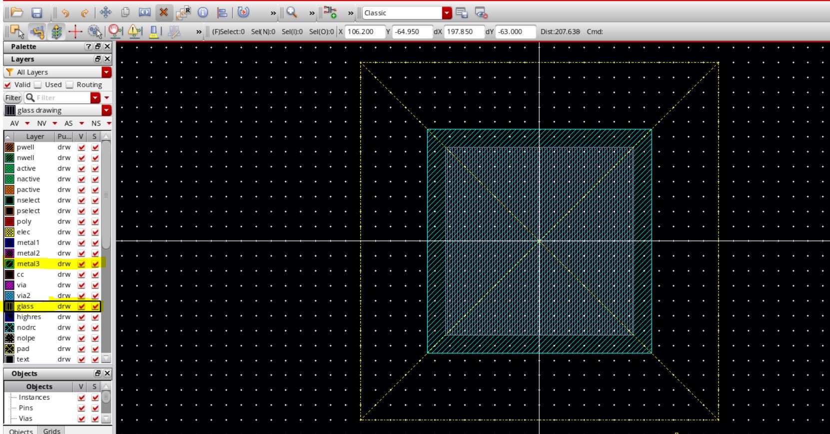
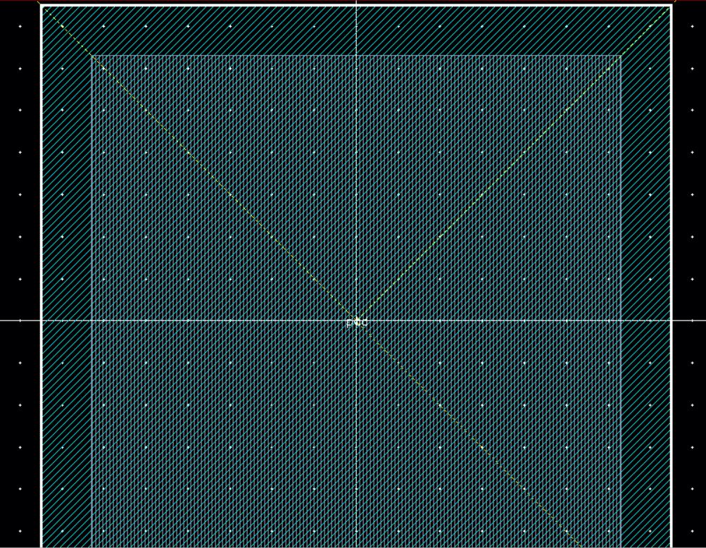
The pad
size is
a metal3 square that is 75 um square and an overglass (called glass)
layer that is 6um smaller or a size of 63 um square. Notice that
both 75 and 63 are divisible by .15, this is to ensure that when we DRC
we have no off the grid errors. Add both of the rectangles
centered around the origin. DRC then save.
Next, add a pin called "pad". The pin will be made out of metal3 and
the
pin's rectangle will cover the original metal3 square. The pin
will have a direction of inputOutput.
Select the pin name and set its height to 18 um.
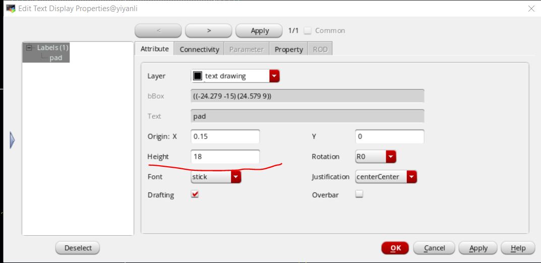
DRC and save the layout.
Next create a new layout cell called "padframe" and instantiate the pad
cell into it.
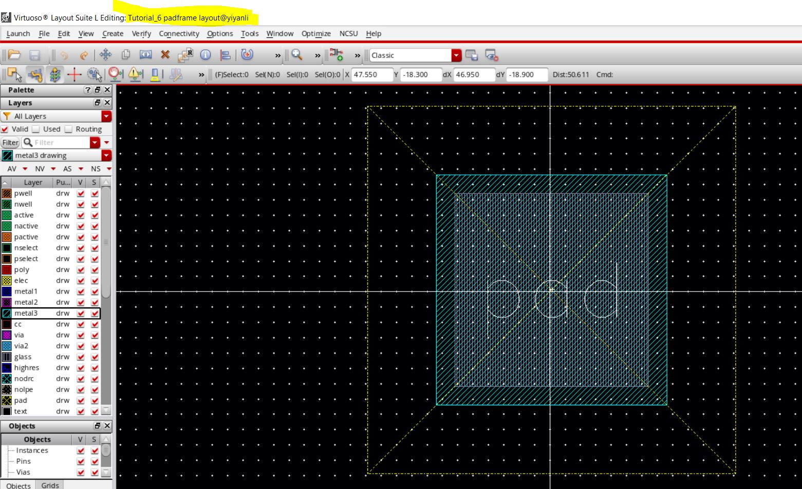
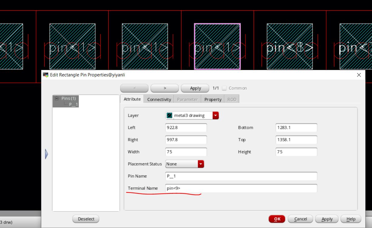
Make a pin out of the metal3 layer called pin<1> with a direction
of inputOutput. Make the pin the same size and the metal3
layer. Ensure that Display Pin Name is selected. Then set the
text height to 15 um.
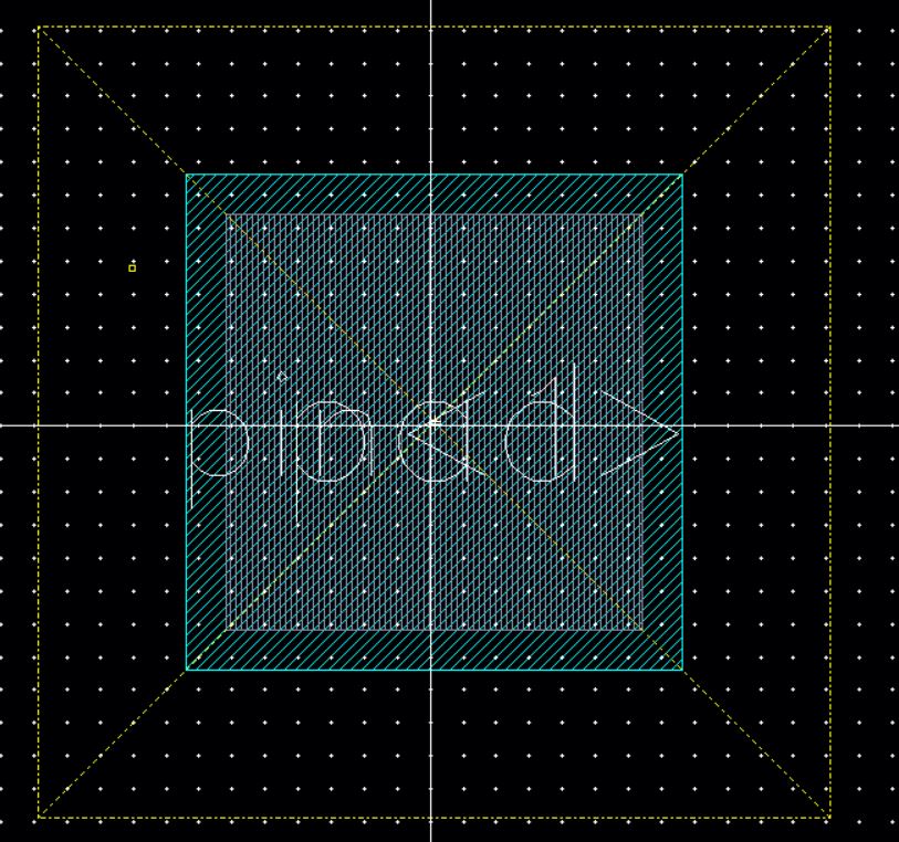
It will look something like this:
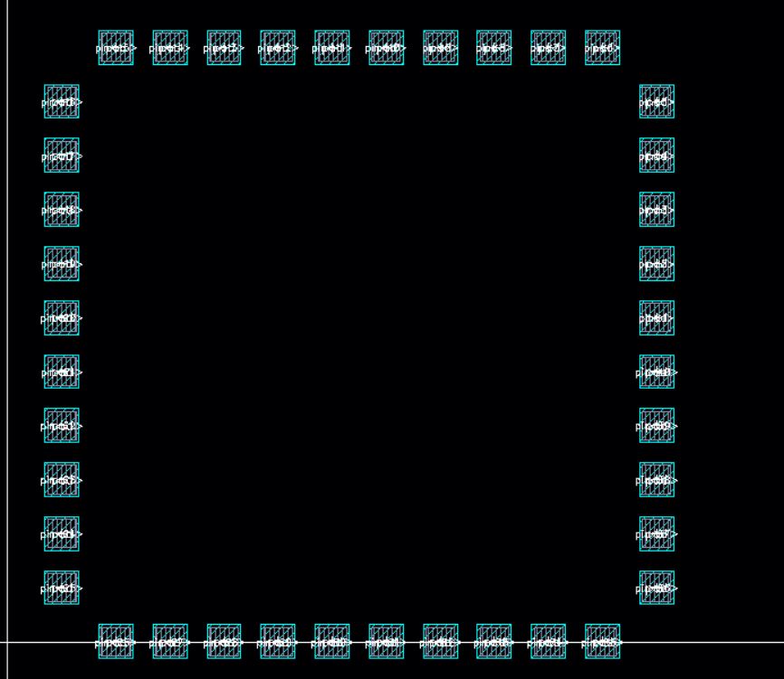
Next copy the pad and the pin, the set the number of rows and
columns to 12.
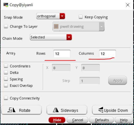
Then click on the lower left hand corner of the layout.
Next, click on the lower right hand corner of the layout.
This ensures that the new cells are aligned.
Then drag the copies horizontally and when they are aligned perfectly
click. Finally click on the top right hand corner of the original pad.
This will align the copies vertically.
Its ok to make mistakes, to try again just hit "u".
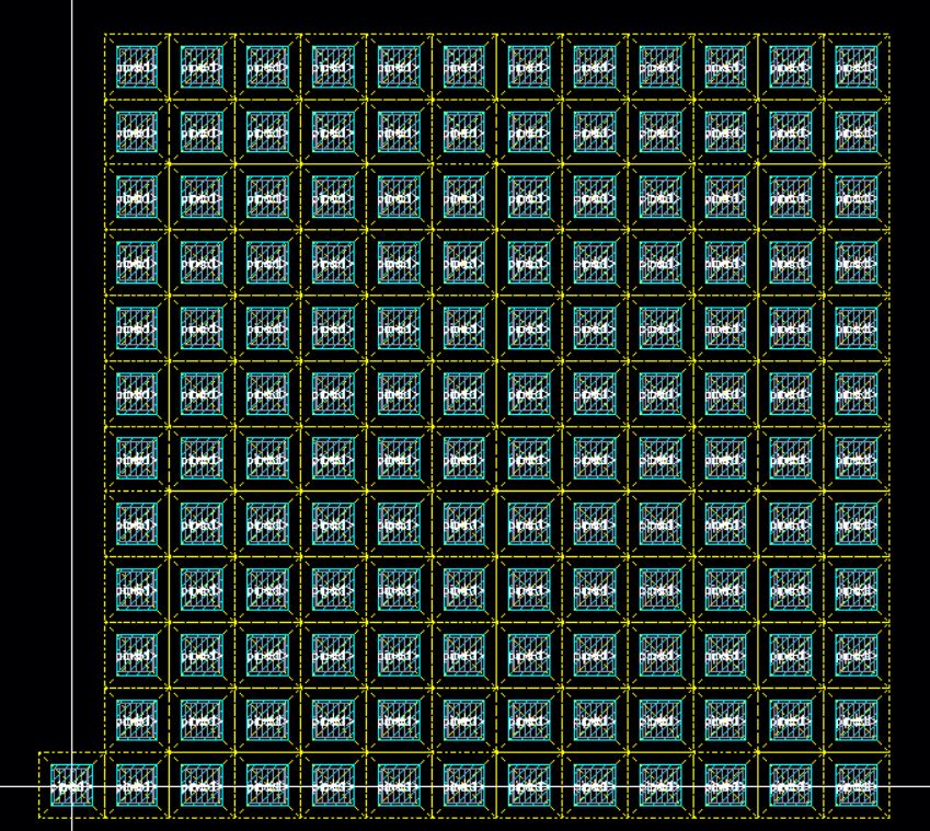
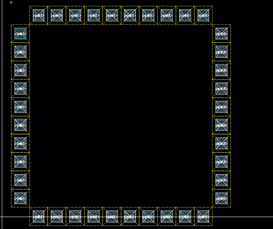
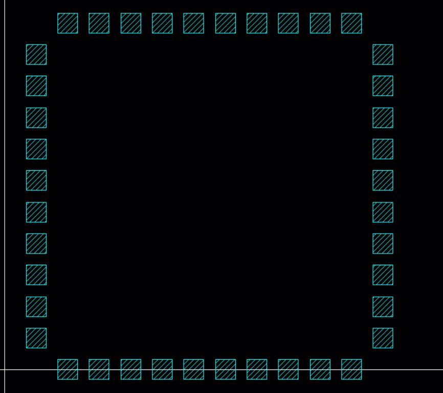
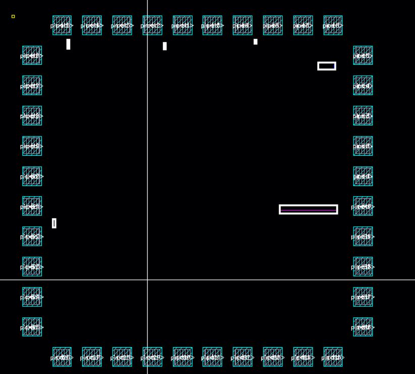
Delete the middle, corners, and extra pads/pins to get the basic
padframe seen below.
DRC and save the layout of the padframe.
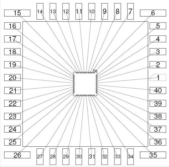
The padframe is likely bonded to the package with the configuration
seen below (the bonding diagram).
All of the pins in the above layout are labeled pin<1>. Change
the labels so that they match the bonding diagram seen below. For
example, pin 1 of the package corresponds to the 5th bonding pad from
the top on the right side of the die.
To make this go a bit faster set your display level stop to 0.
In order to change the name you have to click on the metal3 not the
text. This will take a moment. When you are finished DRC and
save.
Next delete the pad layer from the pad layout cell. The yellow
boxes will disappear from the pad frame layout.
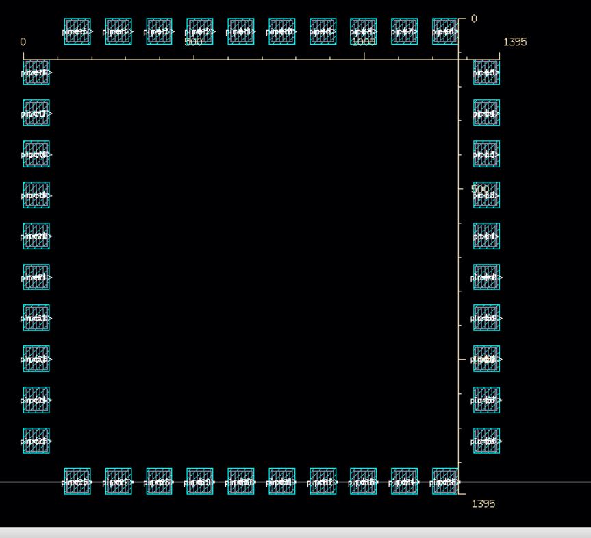
Let’s measure the size of the padframe (our chip) since we’ll need this
information if we submit to MOSIS. To use the ruler press "k" .
Using the ruler we get the following sizes (1.395 mm square).
Now generate an extracted view, then open it.
We now need to make the schematics for the pad and padframe layouts.
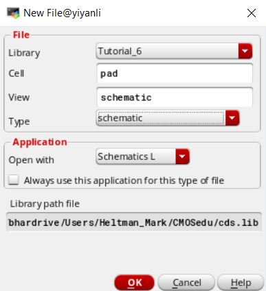
Make a schematic cell view in pad. Add a pin called "pad" with a
direction of inputOutput.
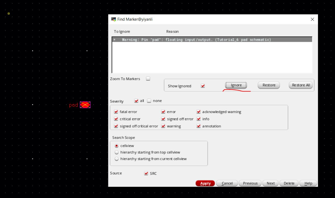
Check and Save the schematic.
Ignore the warning that the pin is floating.
Check and save the schematic again.
Note that an LVS can't be performed between the pad schematic and
layout since there are no devices (resistors, capacitors, transistors)
in the circuit.
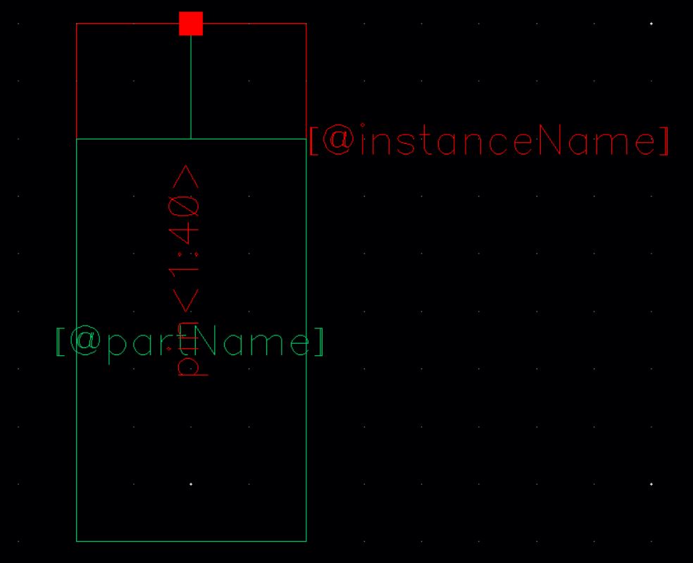
Now create a new cell view from the current one. To create a
symbol for the pad.
Delete everything except the green box and the label "pad". Then rotate
the box, and save.
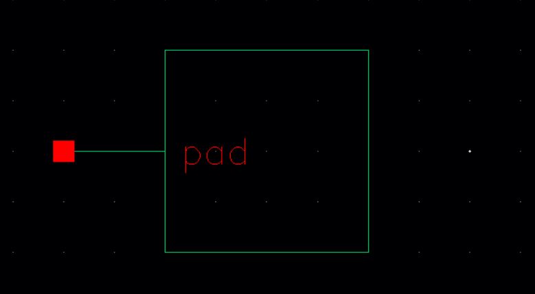
Close and save.
In padframe create a new schematic cell and place in it the pad cell
symbol.
Then add an array of 40 to the name of the cell.
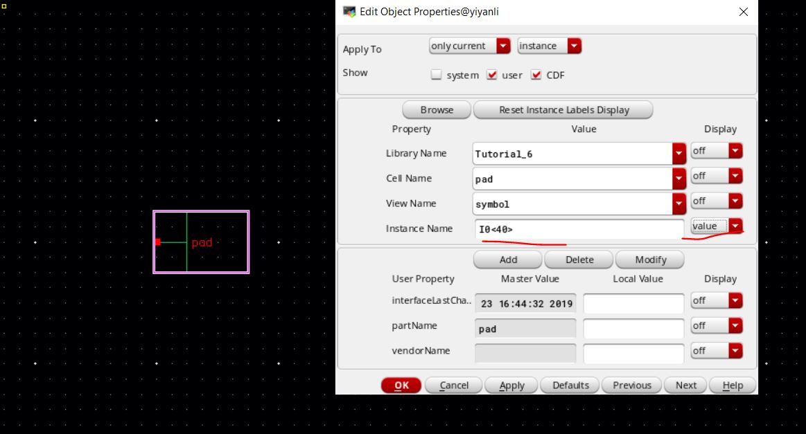
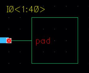
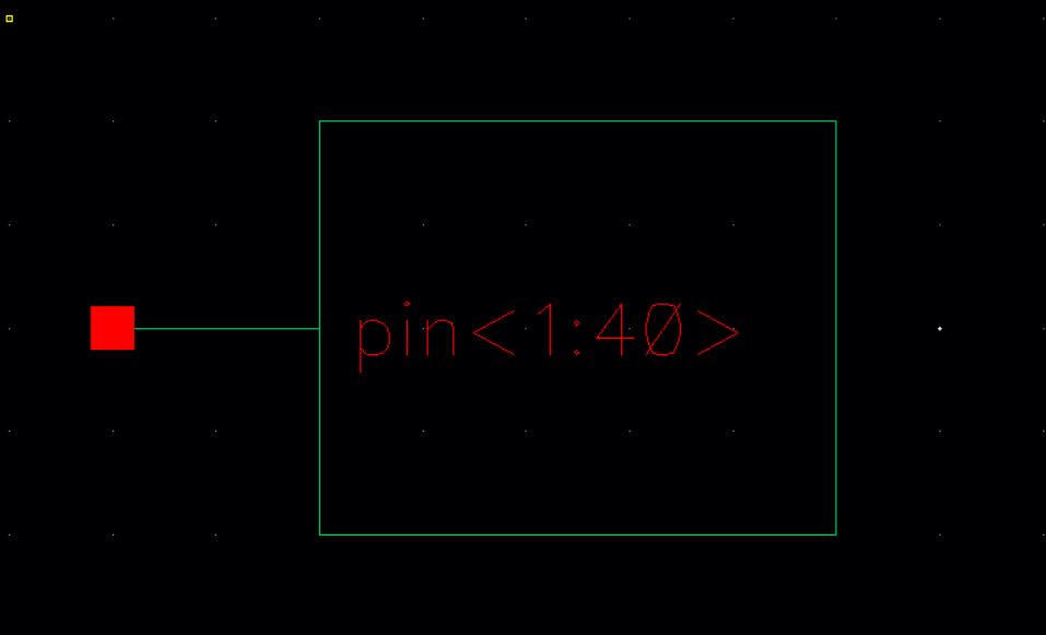
Add a pin with a name of "pin<1:40>" with a direction of
inputOutput. Connect the pin and pad with a wide wire and label
it
"pin<1:40>". check and save the schematic.
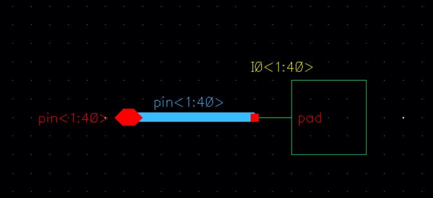
Now let's create a symbol for the padframe. Create a new cell
view
from a cellview.
Create the following symbol.
We are now ready to create our chip layout.
Create a new schematic cell view called "chip" and add all the symbols
we have created to it.
Add wires and label them as below the connections are arbitrary.
Note how we’ve used pin<20> for ground and pin<40> for
power(label on thick wire)
Don't forget to add vdd and gnd.
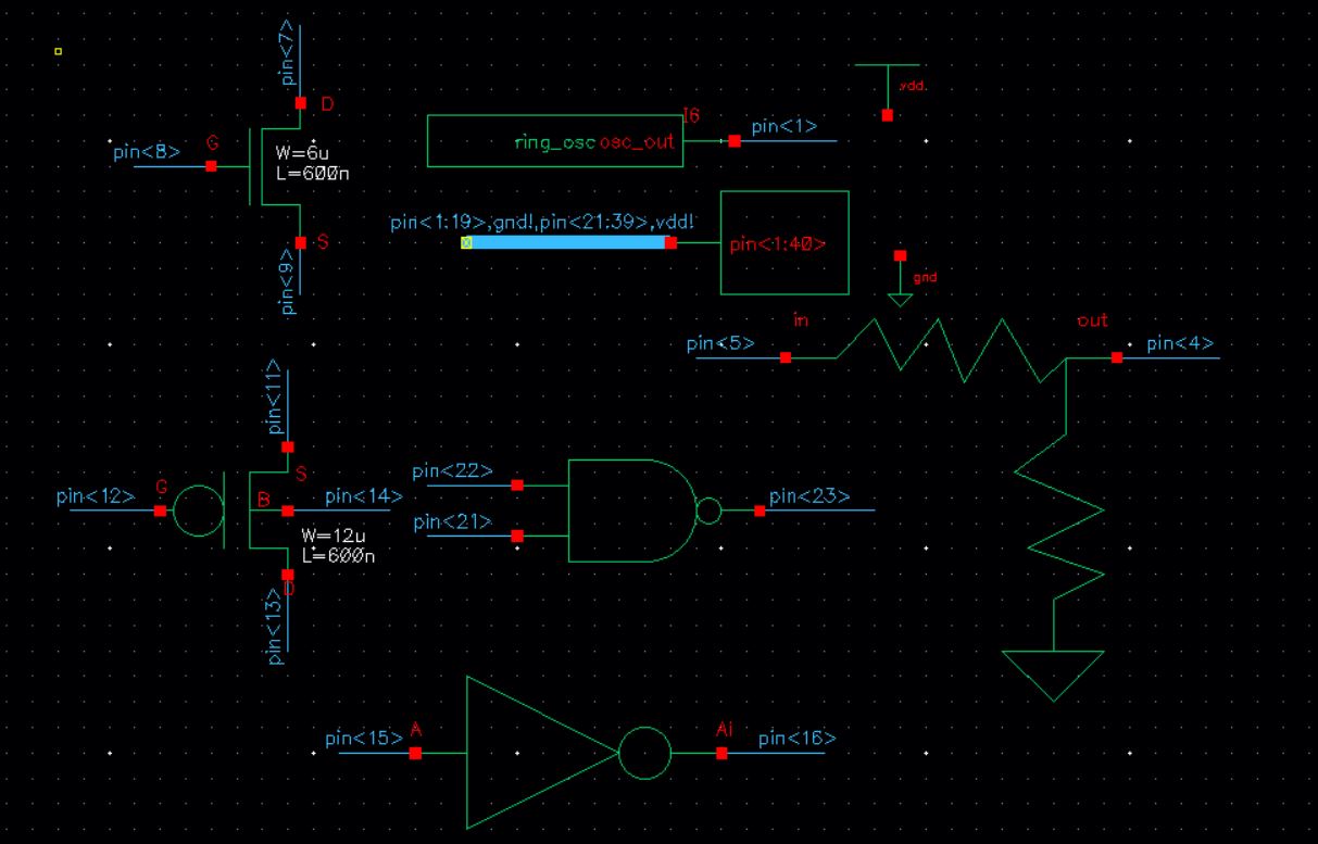
Check and save, you might have to move some parts around.
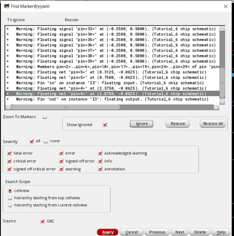
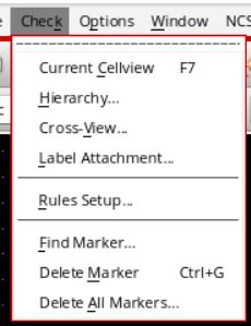
Ignore all the warnings then check and save again. If the warnings
reappear mouse over to "Check" then click on "Rule Setup"
In the popup window change Floating Nets to "ignored"
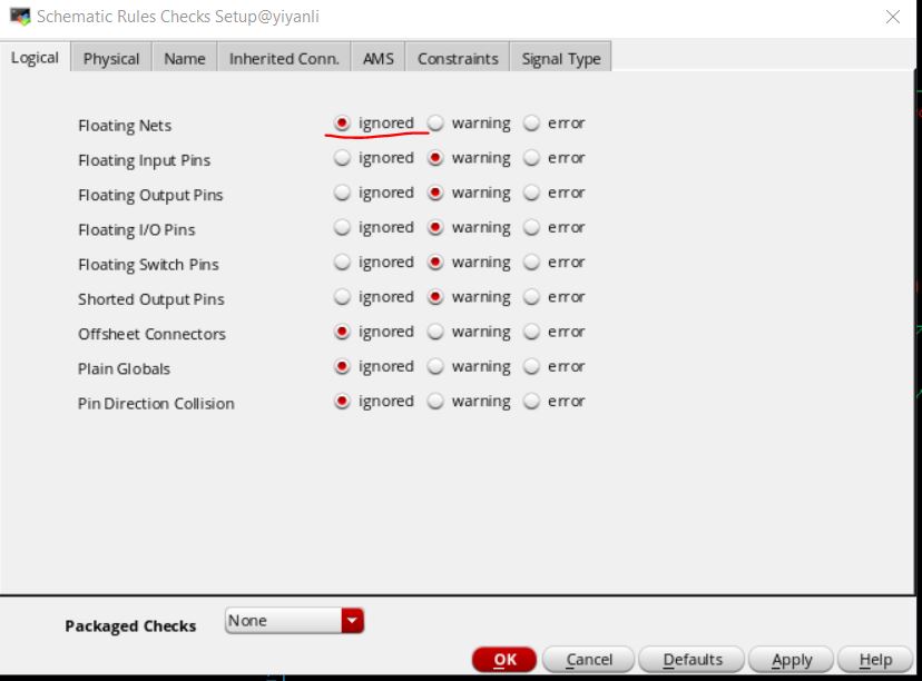
Then check and save.
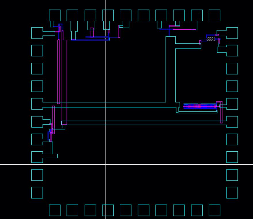
We are ready to connect the cells up to the padframe in the layout.
Create of layout view of the “chip” cell.
Place the R_div, NMOS_IV, PMOS_IV, inverter, nand2, and ring oscillator
cells near the pads that they will connect to, below.
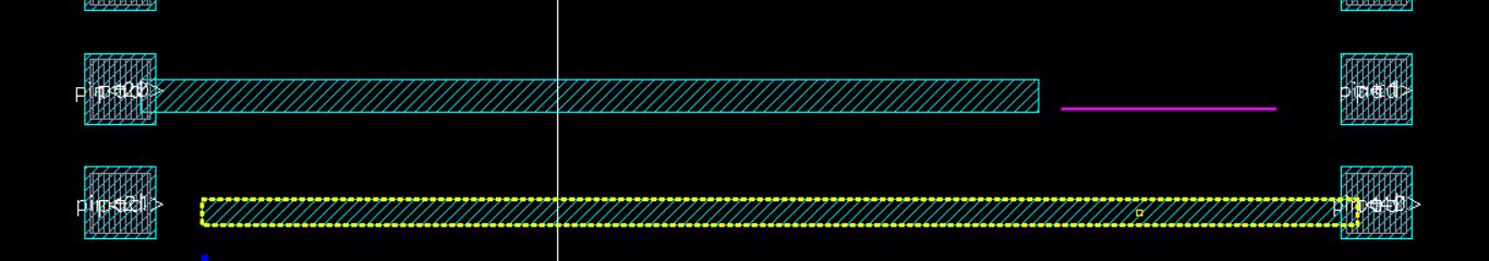
Draw a metal3 connection starting at pin<40> almost to the other
side. This will be our power in.
Then draw a metal3 from pin<20> and going almost to the other
side. This will be our ground.
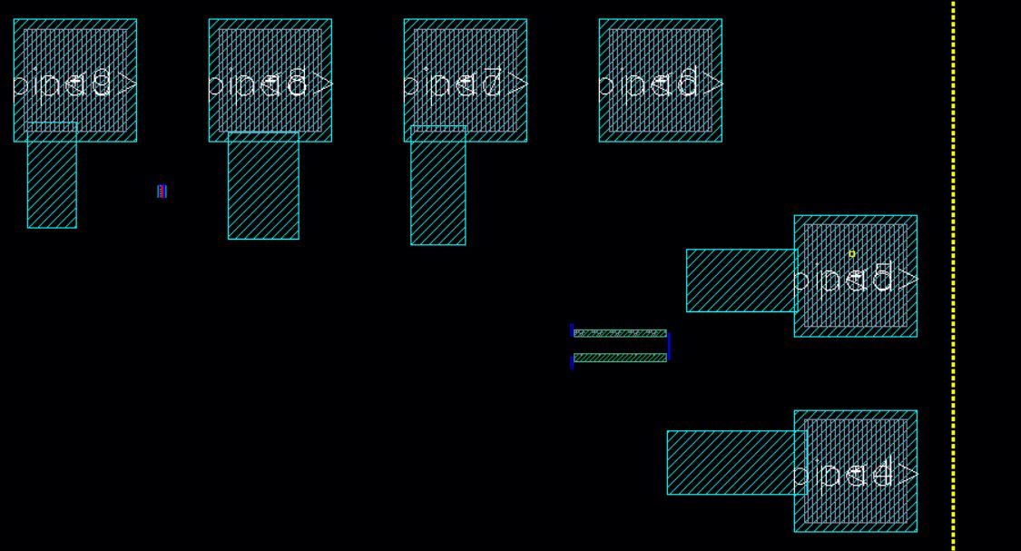
Next draw the metal3 connections from the pins you selected in the
schematic. It does not have to be pretty. For example
below I have drawn the metal3 connections for the voltage divider and
for the nmos.
DRC and fix any errors.
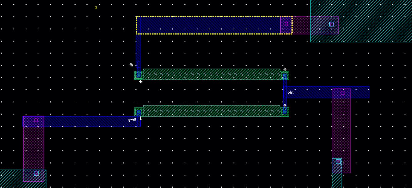
Next, start to wire your connections.
Metal1 connects to metal2 which connects to metal3. However the
metal2 can crossover metal3. Each one of the layers is on a
different level. We will connect the levels later.
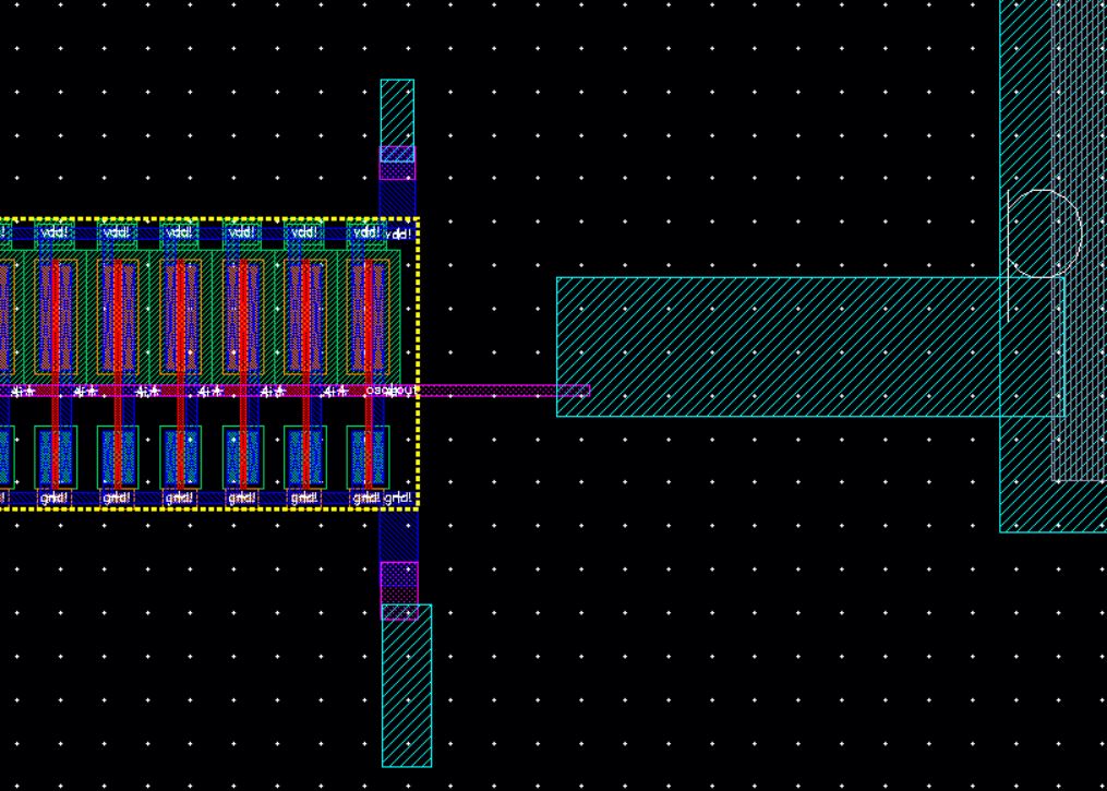
For example here is the ring oscillator connections.
Voltage divider
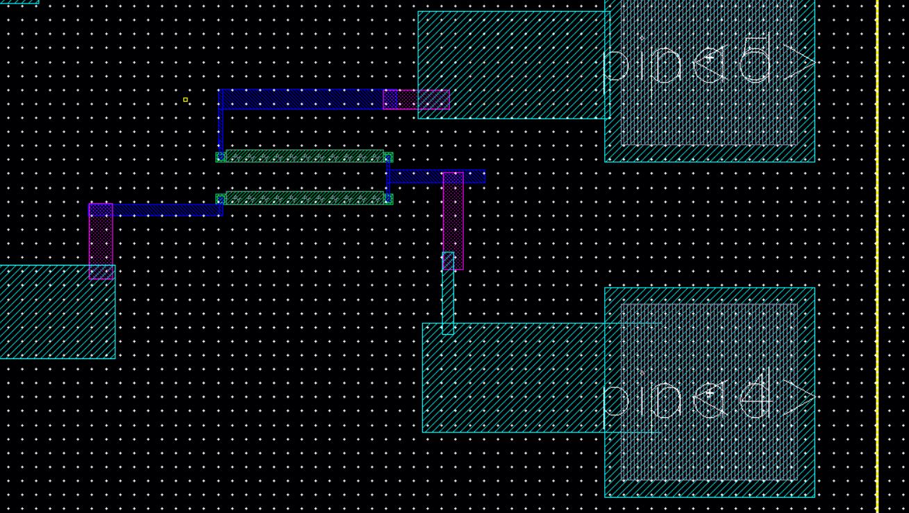
Nmos
Continue to wire up the rest of the components. DRC after each
on. Then, save.
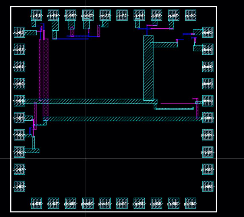
Your finial drawing might look something like this:
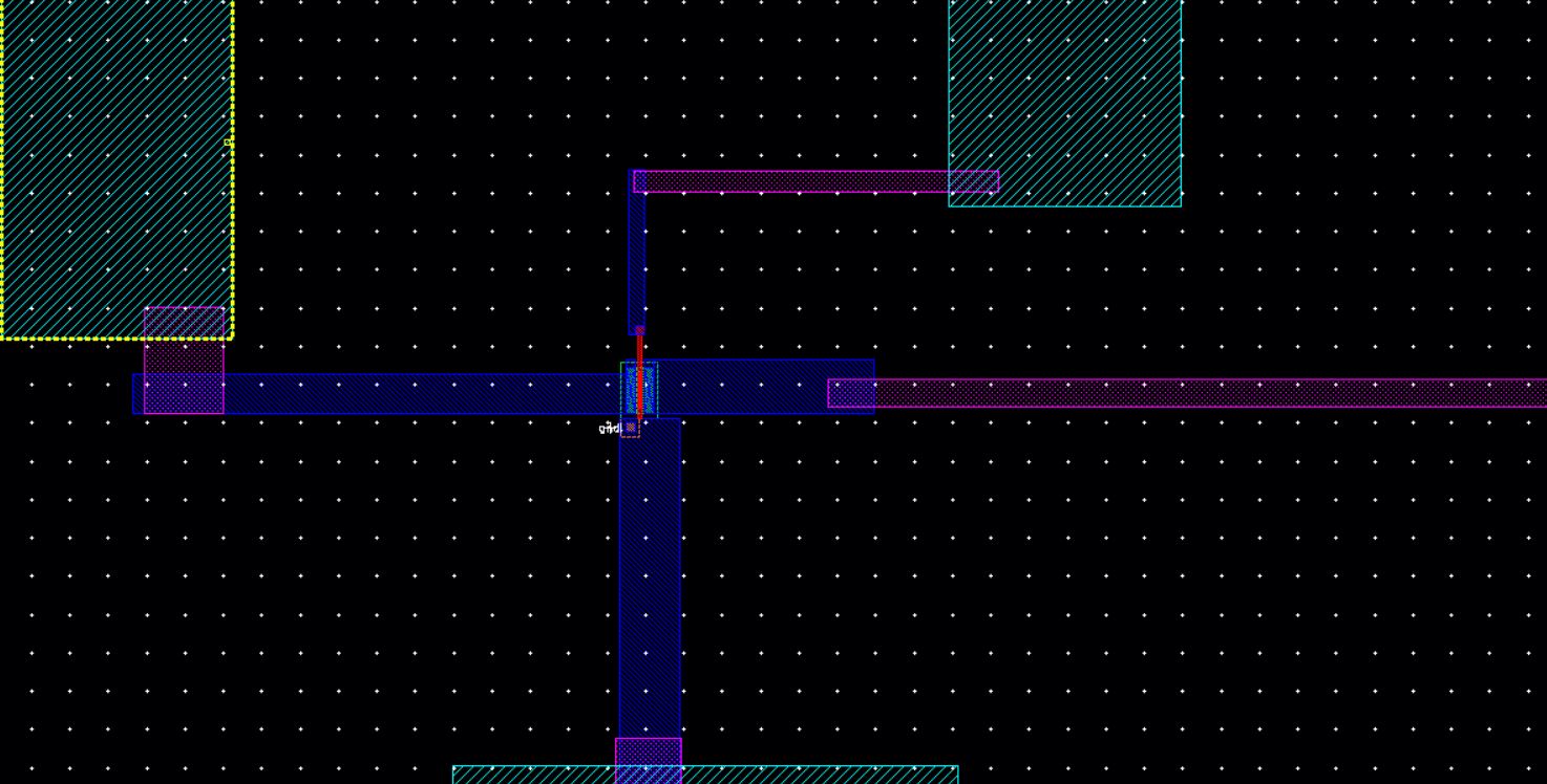
Now we are going to add the vias. They are m2_m1 and m3_m2.
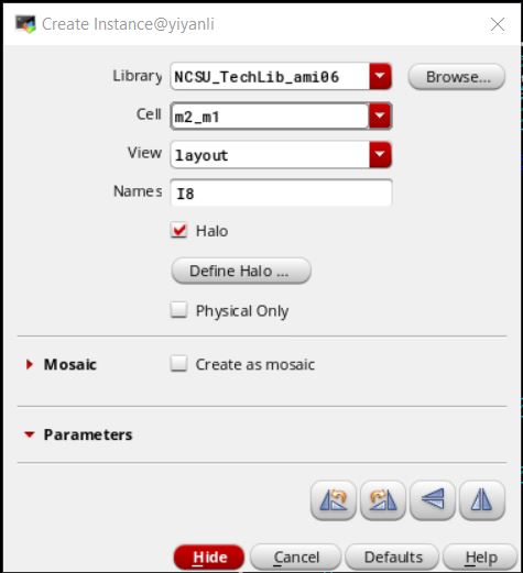
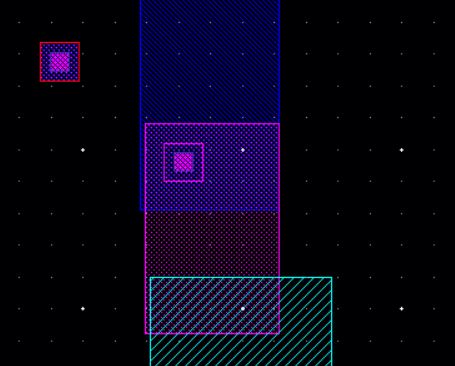
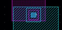
Below are some finished
examples.
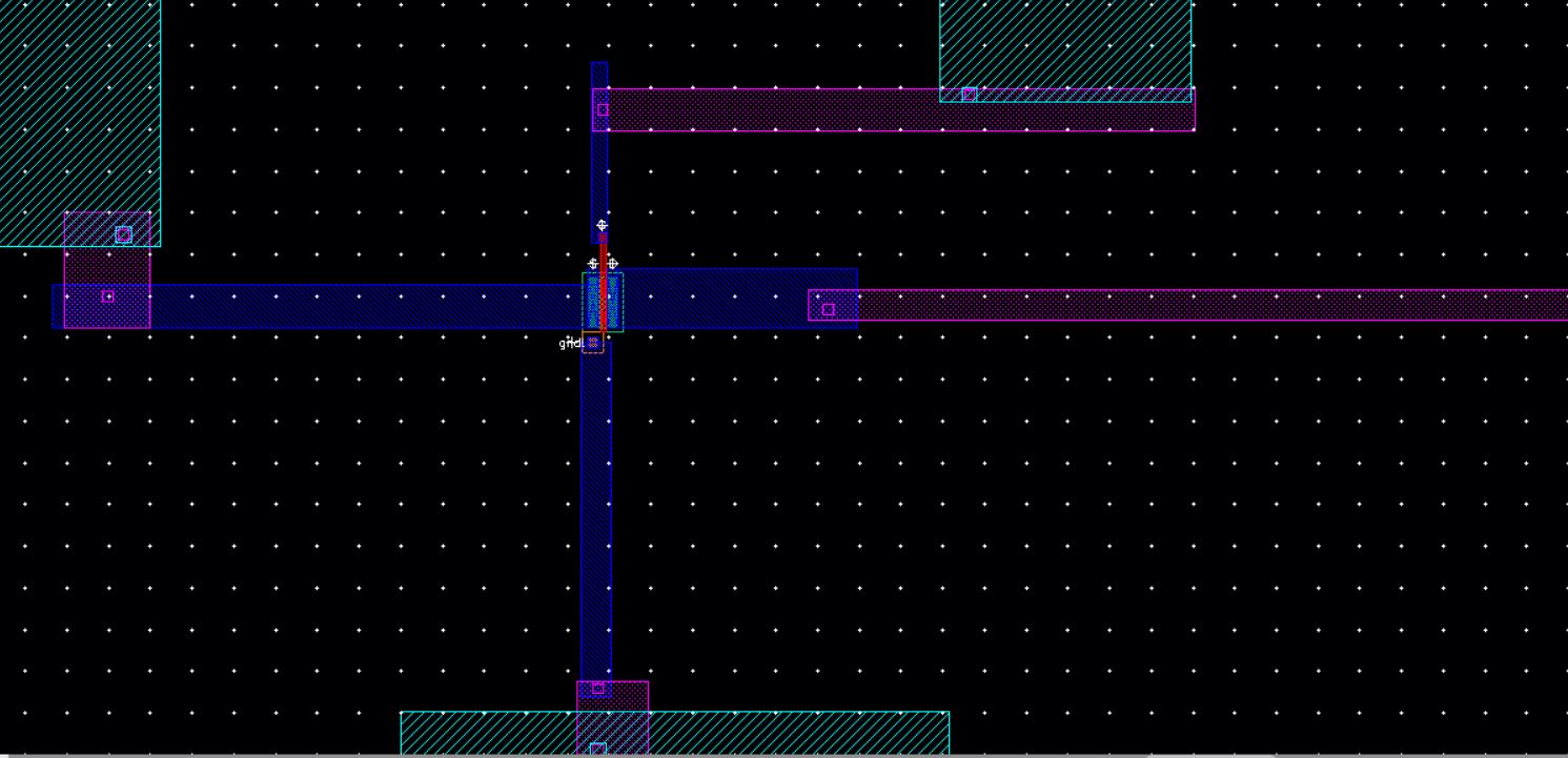
Add vias to the rest of the layout. DRC and save. after adding
the vias extract the layout.
Finally run and LVS.
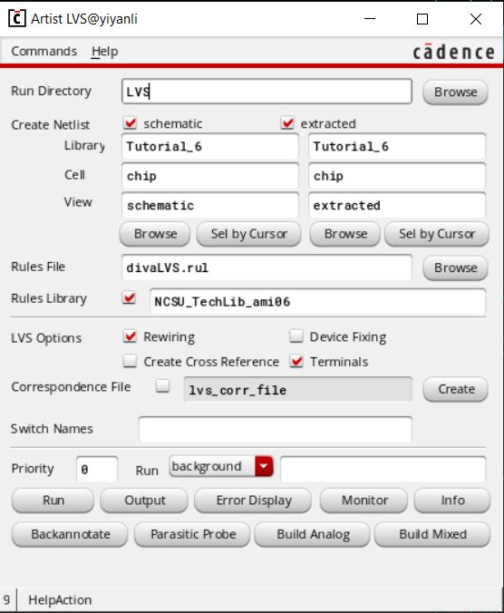
To help fix LVS errors click on "Output" and scroll down to view
errors, or click on "Error Display" and change the display to
white.
When the netlists match...Congratulations you have finished
tutorial 6.
.