Tutorial
2:
NMOS and PMOS
This tutorial assumes that you know the necessary basics from the
first tutorial.
Start Mobaxterm and login to the server, navigate to CMOSedu and
start virtuoso.
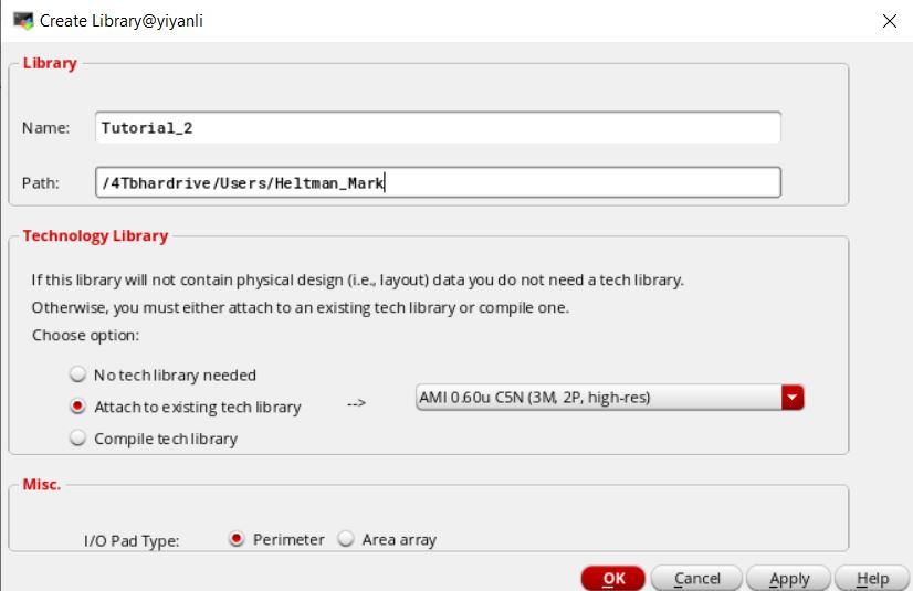
In the library manager go to file, new then library. The library name
will
be Tutorial_2. Use the same tech library as last time.
Copy everything in Tutorial_1 into Tutorial_2. To do this right click
on Tutorial_1 and click on copy. In the pop up window set the “to”
library to Tutorial_2. under options make sure that "Update
Instances" is checked. Then press ok.
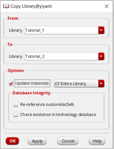
If another window pops up just press ok.
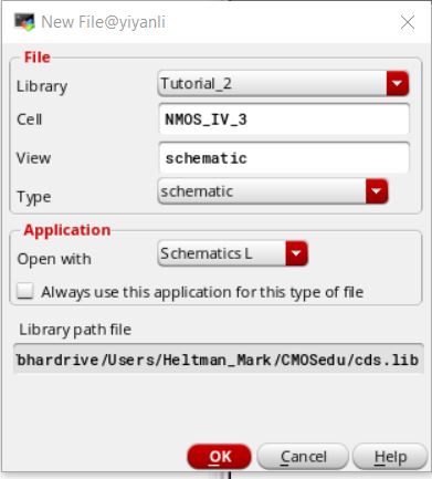
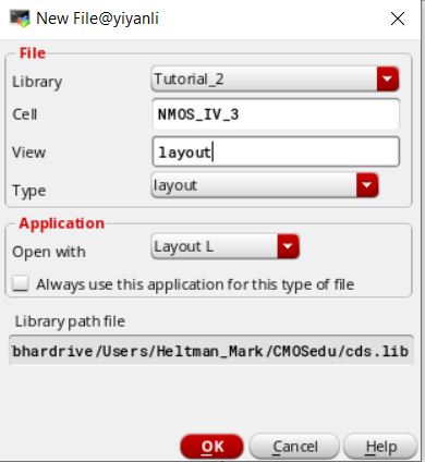
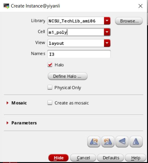
With Tutorial_2 highlighted go to "File" then "New" then "Cell View"
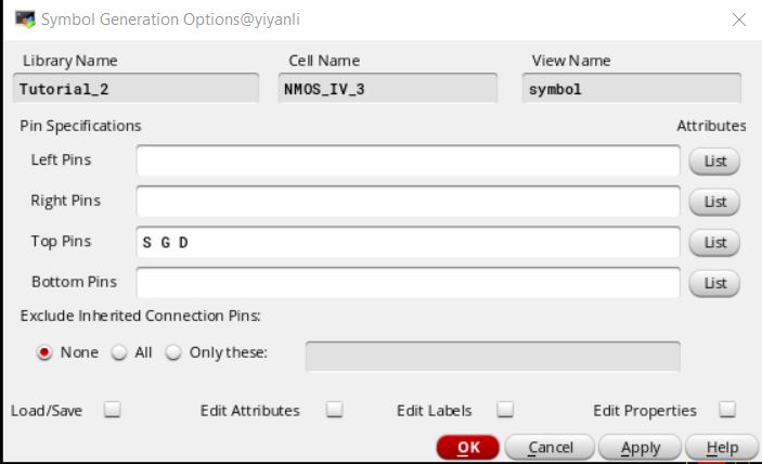
Name the cell NMOS_IV_3 the 3 indicates that this will be a three
terminal component. Make sure that the view is schematic.
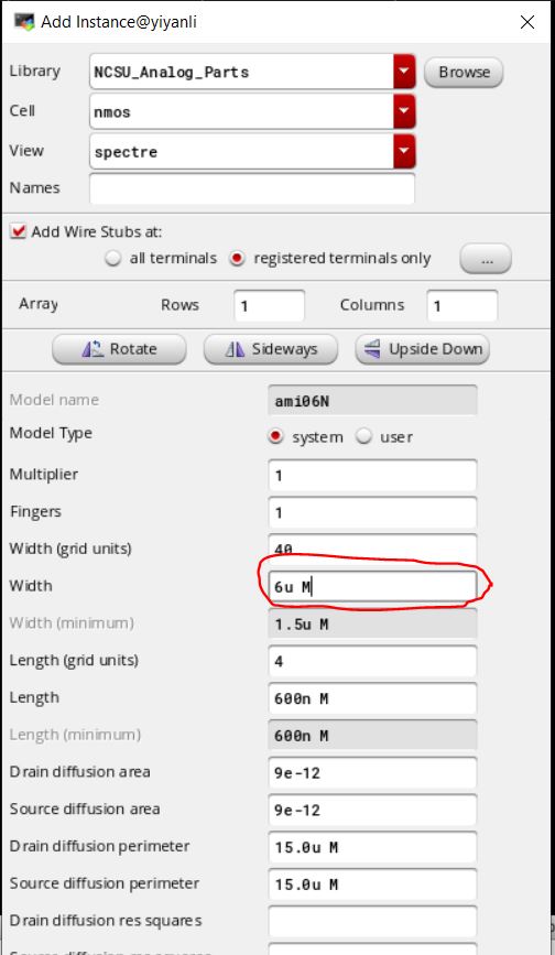
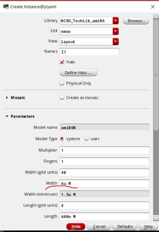
In the Schematic editor press "i" and change the cell to nmos, the
library is NCSU_Analog_Parts, set the view to symbol
change the width to 6u. Then place the part.
Add pins and wires to the schematic. The pin direction should be
inputOutput. The name of the pins will be "D", "G", and "S". Right
click to change to orientation of the pins. When finished
check and save.
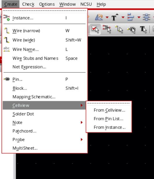
Next we are going to create a symbol view for the schematic. Mouse over
to "Create" then to "Cellview" then to "From Cellview". Press
"ok" on the first window. In the second window press "ok " ,
because we are going to change the pin configuration anyway.
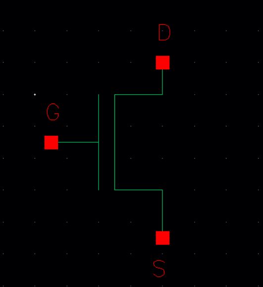
Like last time delete everything accept the pins.
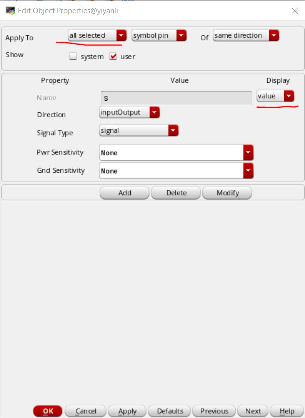
We cannot see the pin names, so select all 3 pins then press "q" to
edit the properties.
Change "Apply to" to "all selected". Then change the "Display"
to "value". Then press "ok"
Move and rotate the pins to draw a MOSFET symbol. Draw lines by
going to "Create" then to "Shape" then to "Lines"
When you are finished check and save.
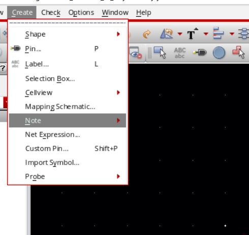
We are going to add text to the symbol so we know the length and the
width. To do this mouse over to "Create" then to "Note" then to
"Text".
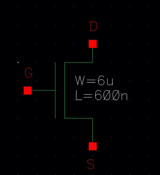
The note should say W=6u and L=600n. Place the note close to the
symbol. When its place check and save.
Close out of the schematic and the symbol, return to the library
manager.
Now we are going to simulate the NMOS.
In the Tutorial_2 library create a new schematic cell called
sim_NMOS_IV_3. In the new Schematic place down the NMOS symbol that we
just created. To do this press "i" and change the library to
"Tutorial_2", the cell to "NMOS_IV_3"
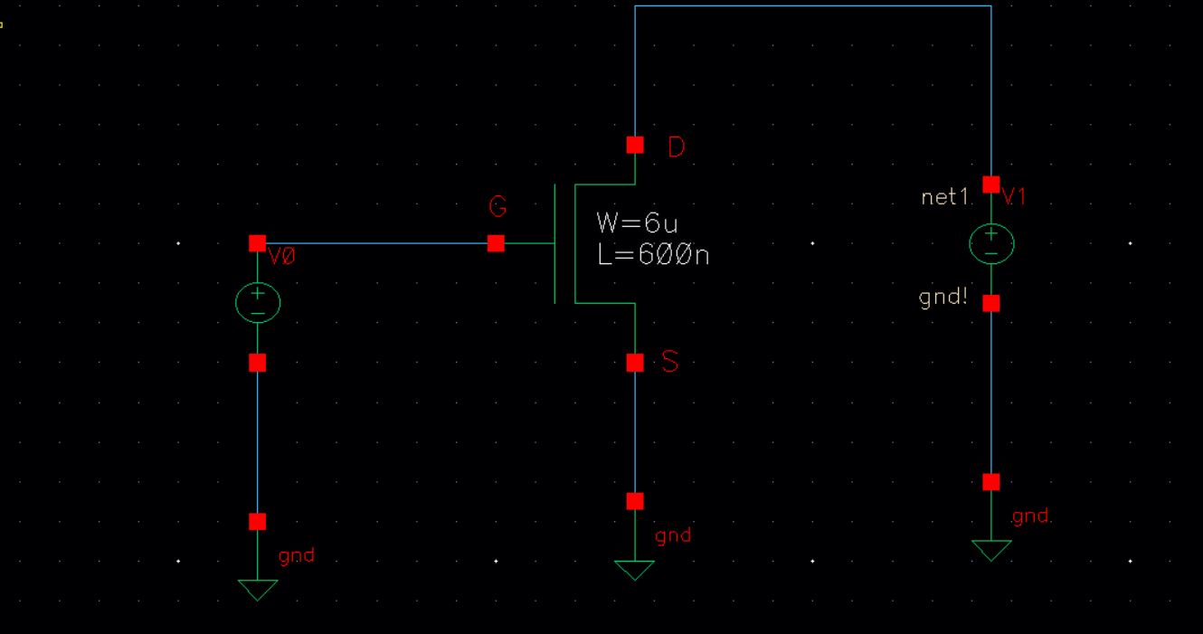
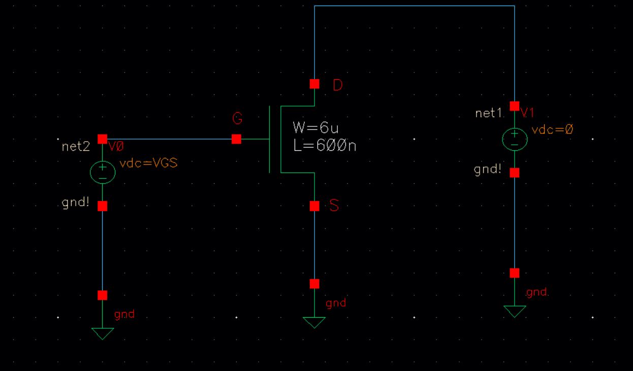
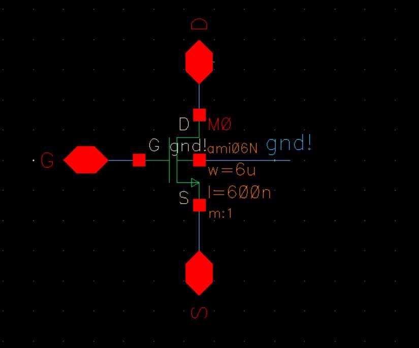
Then add form the NSCU_Analog_Parts library vdc power and gnd. Wire it
all up to look like the following: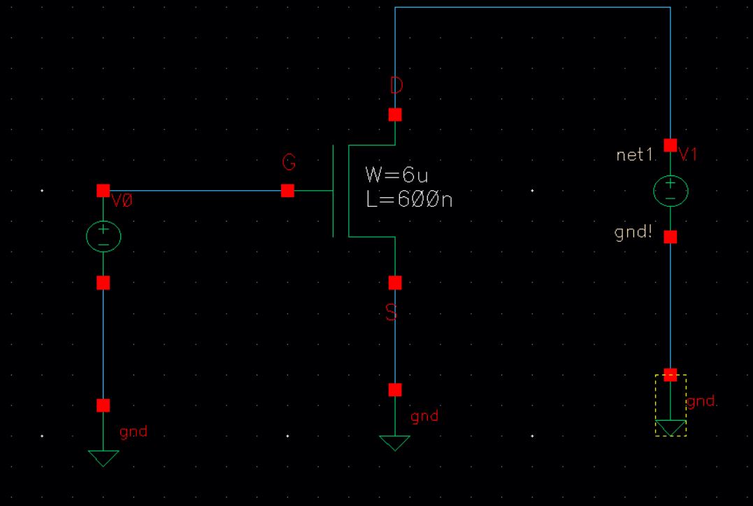
Notice how the S is upside down, and how both the S and D are in the
way
of the wires? To fix this open the NMOS symbol and click on the letter
and press "m". While in the move mode right click to rotate the
symbol. When you are finished check and save, then close the
symbol view.
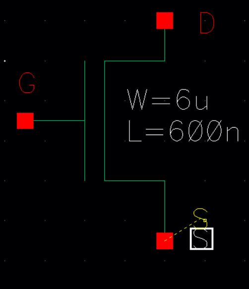
Now the letter have moved on the schematic.
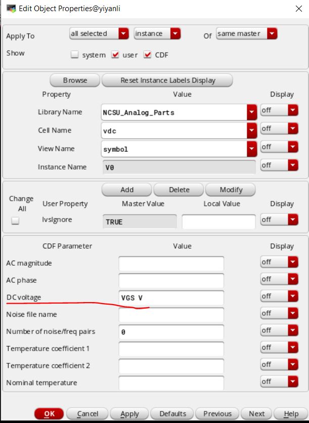
Set the value of V0 to "VGS" and set the value of V1 to 0. Then check
and save.
Now launch ADE L.
Change the simulator to spectre as done is the last tutorial.
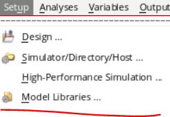
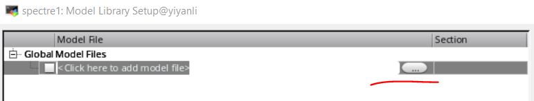
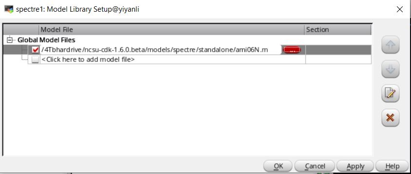
We need to set up a model for spectre to use, mouse over to "Setup"
then to "Model Libraries"
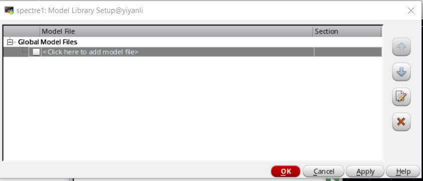
double click in highlighted area unit a "..." shows up then click on
"..."
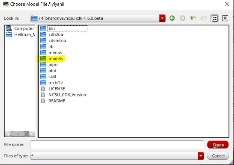
In the new window double click on "models" then "spectre "then to
"standalone". Once in "standalone" select ami06N.m and press
open.
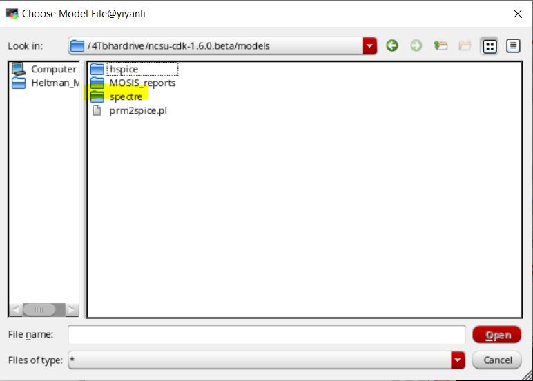

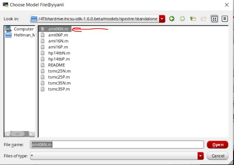
We will have to go through this process again for the PMOS and for the
inverter. PMOS will use ami06P.m. The inverter will use both
ami06N.m and ami06P.m.
Then press "ok" after selecting ami06N.m
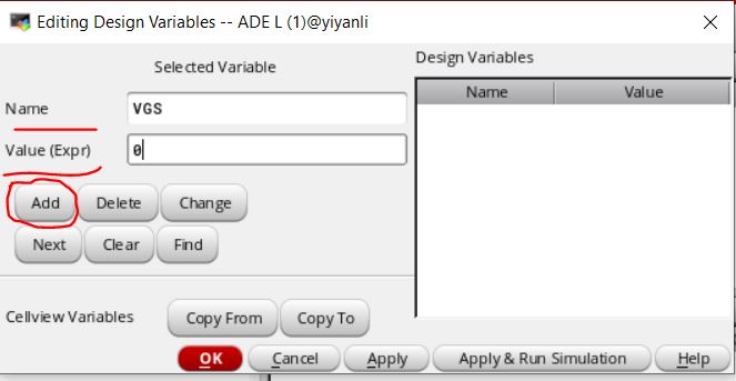
Now we need to set values for VGS. Mouse over to "Variables" and
click on "Edit"
In the pop up window Set the name to "VGS" and the value to 0.
Click add, then "Ok"
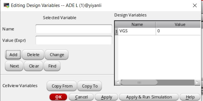
After "Add" is pressed.
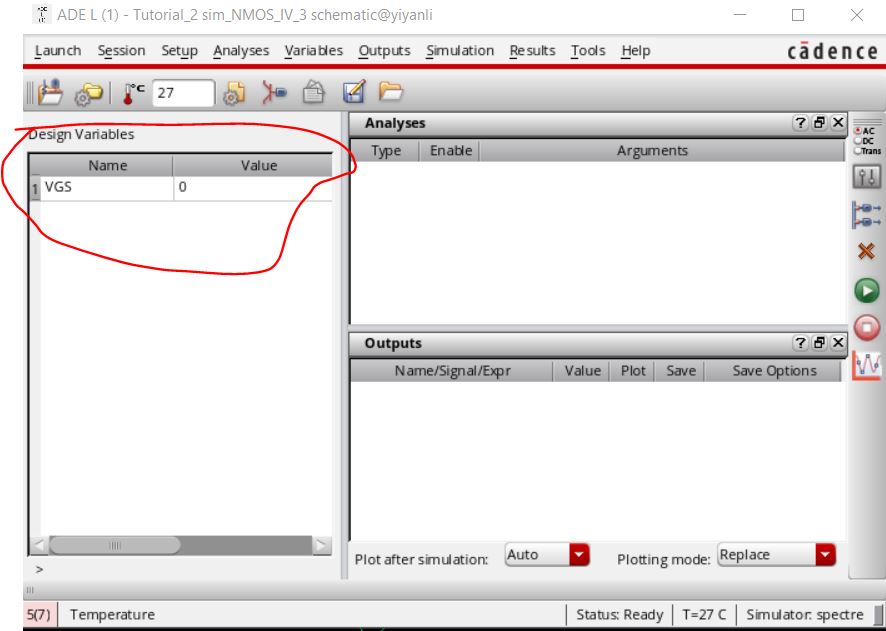
Notice how VGS is now in Design Variables.
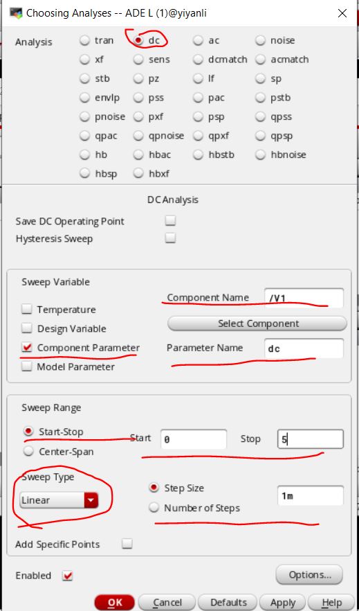
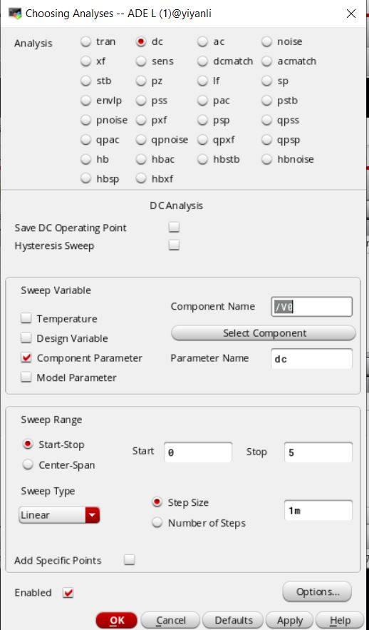
Next select the analyses that need to be conducted.
The type will be dc. Now we need to fill in the parameters
as shown.
Now mouse over to "Outputs" and "To Be Plotted" then
"Select on Design". Select pin "D". Make sure that plot and save
are both check.
Now save the simulation state. Make sure to click on Cellview.
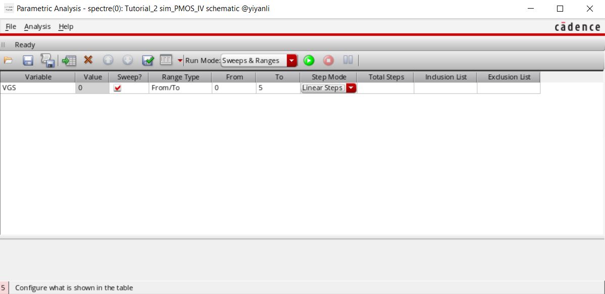
For the last step we need to set up how VGS is going to change.
Mouse over to "Tools" then "Parametric Analysis".
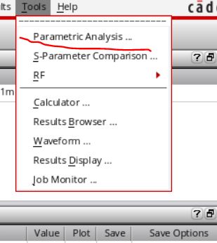
Set the following on the pop up window.
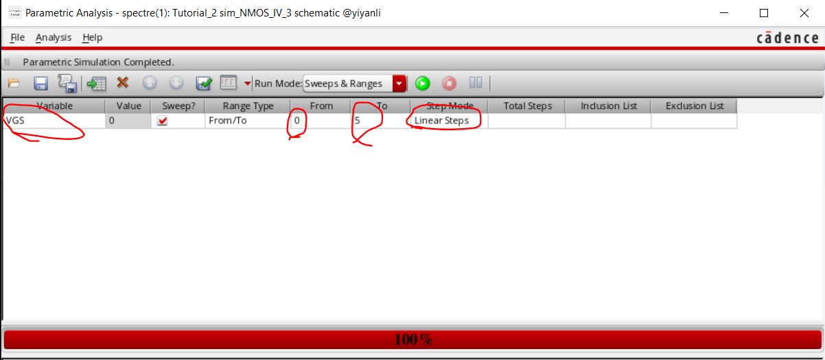
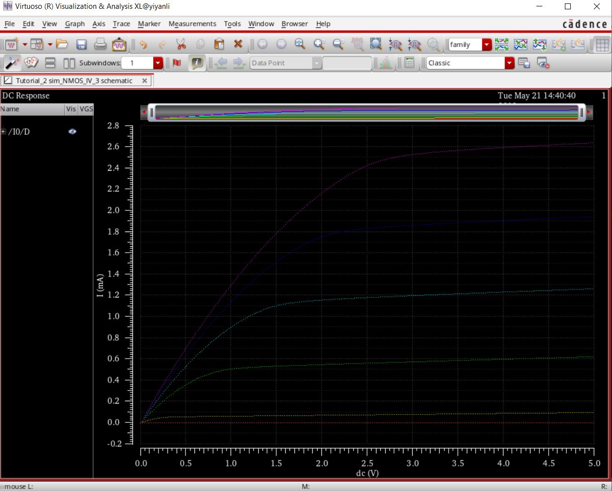
Click run in the Parametric window. This might take a
moment. A plot will come up view the plot it should look
something
like this.
Unfortunately we are unable to save the Parametric Analysis. Save the
State again its ok if it is over written.
Close the ADE and the Schematic used for the analysis.
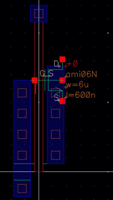
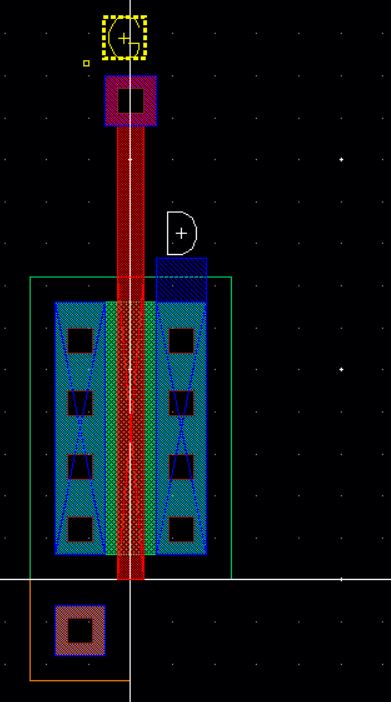
We are now going to create a layout of the NMOS.
In the library manager have NMOS_V_3 selected and then create a new
cell view. Make sure the view type is layout.
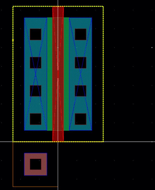
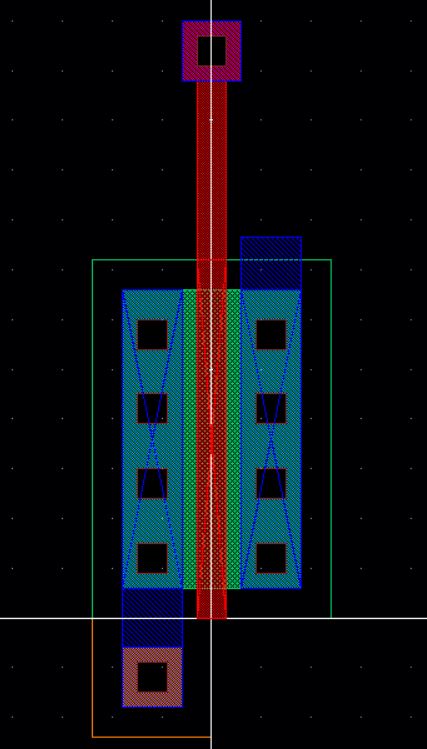
In the layout place an nmos that is 6um wide ad 600nm long.
Now place a ptap. Total is should look like this. Then DRC
and save. Fix any errors that arise.
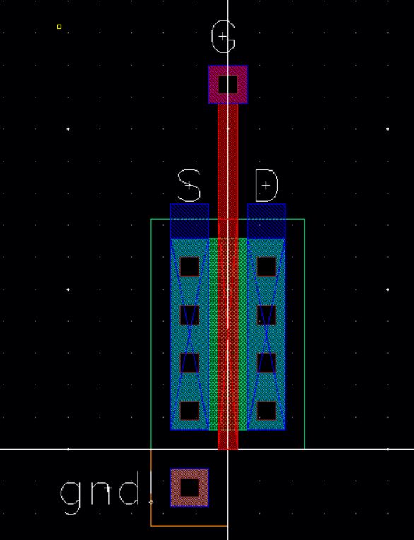
Now add metal1 connecting the ptap and the left side. The metal1 should
cover the entire center of the ptap. Then add metal1 to the right
side on contacts. Select poly and draw out a rectangle upwards
from the center. Then connect the rectangle to a m1_poly.
Then save, DRC and fix errors.
The goal is below.
By pressing "e" and setting the display level stop to 0 we can see the
rectangles we just drew as well as the cells.
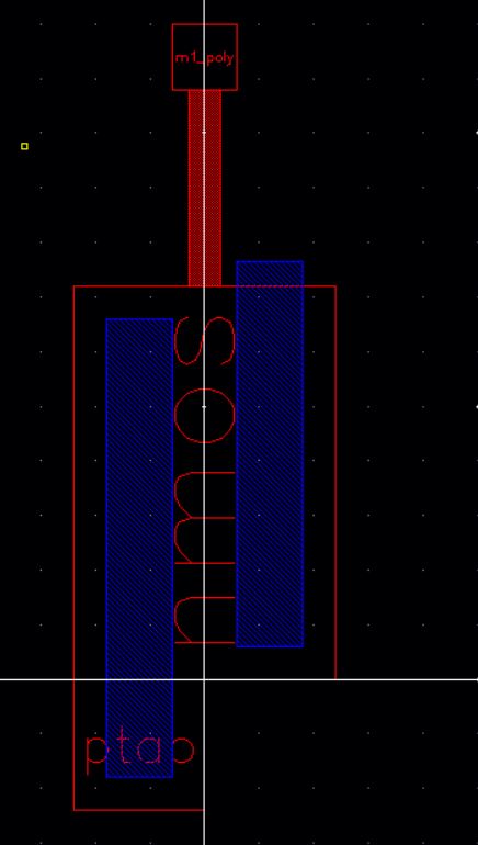
Set the display back to 10.
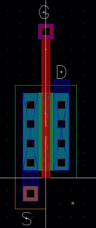
Now add pins "D", "G", and "S" make sure display pin name is selected
and I/O type is inputOutput. Draw the pins so they overlap the
metal1 rectangles.
Save, then DRC, and fix any errors.
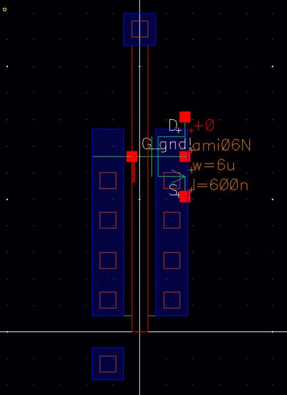
Now extract the view and open it.
Notice that the symbol displayed here has 4 terminals, not the
3-terminal transistor we used in the schematic (where it’s assumed the
p-substrate is tied to gnd!)
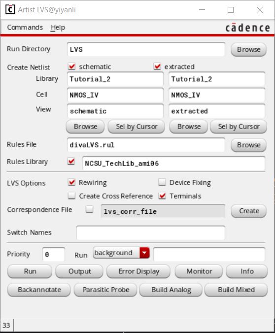
Now run an LSV.
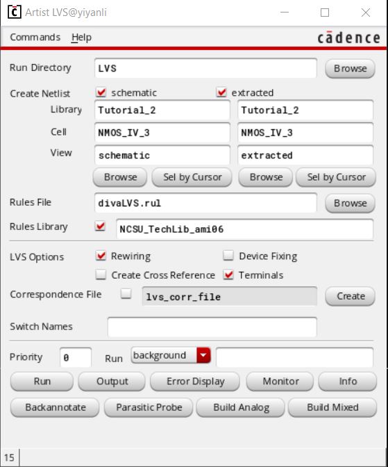
After its runs we notice that it fails. Click on "Info" if
a
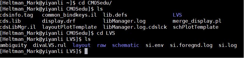
window does not pop up go to mobaxterm and navigate to the LVS folder
in CMOSedu. Then use nano to open si.log.
si.log is the LVS log. In the file scroll down until you find the
error: Could not determine the node name for terminal 'progn(bn)'
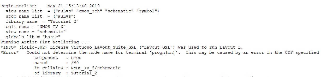
The error is related to the bulk (p-substrate) connection for the NMOS.
Again, as mentioned above when the 3 terminal MOSFET symbol is used
it’s assumed that the ptap is tied to gnd!(global ground)for an NMOS
device. And vdd! for a PMOS device.
Close the extract view and the LVS window.
We are going to modify the layout; Delete the metal1 and pin S that
connect the left side to the ptap.
Now add metal over the ptap and the left side. Then add pins the
same size as the rectangles. Save then DRC and fix any errors.
Now make a new extracted view, and open it.
Notice that it’s basically the same view except that now the ptap of
the NMOS devices is connected to gnd!
Now try and run a LVS.
We see that it fails.
We still have to fix the schematic view, Close out of the layout and
the extracted view.
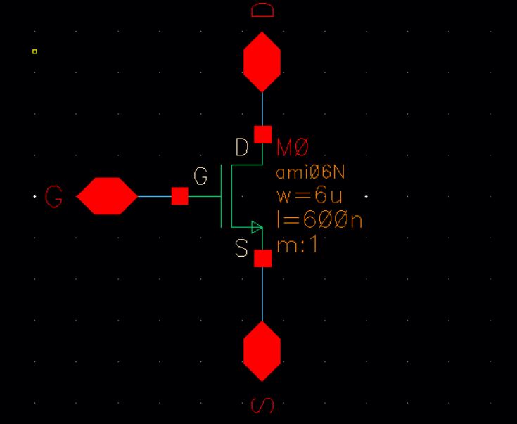
In the Library Manager and rename NMOS_IV_3 to NMOS_IV, rename
sim_NMOS_IV_3 to sim_NMOS_IV
If it does not work, they can be renamed at a later date by closing
then reopening cadence.
Open the schematic in NMOS_IV. There change the cell name to
nmos4.
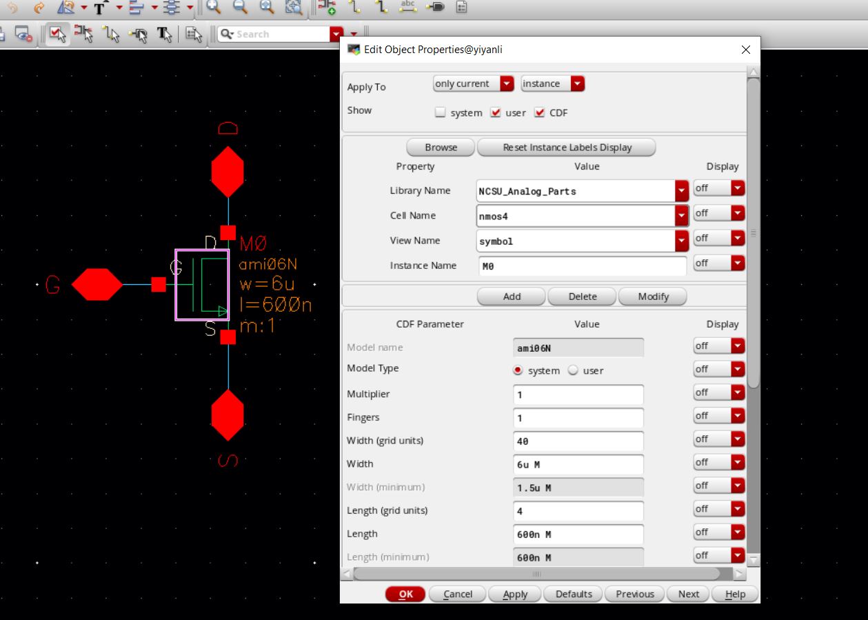
Move the symbol back into place then add the wires and labels as seen
below.
It will be good practice to simulate the updated schematic using the
sim_NMOS_IV. Following the steps above to ensure that we still
get the same plots.
Open the extracted view and run LVS.
As we can see the LVS succeeds !!!!
Now we are going to simulate the extracted layout view.
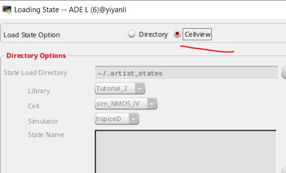
Open the schematic view of sim_NMOS_IV and open ADE L. In ADE click on
"Session" then "Load State" load state from cell view.
Double check that spectre is the simulator
If a plot appears close it.
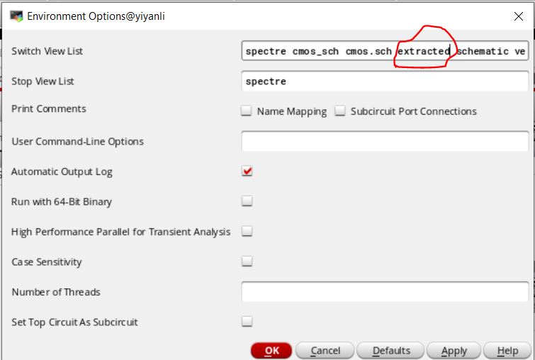
Now in the ADE window click on "Setup" then click on "Environment"
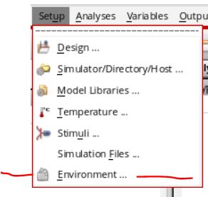
In the pop up window type "extracted" before the schematic in the
switch View List. Then press ok
As we had done before set up the Parametric Analysis and run the
simulation.
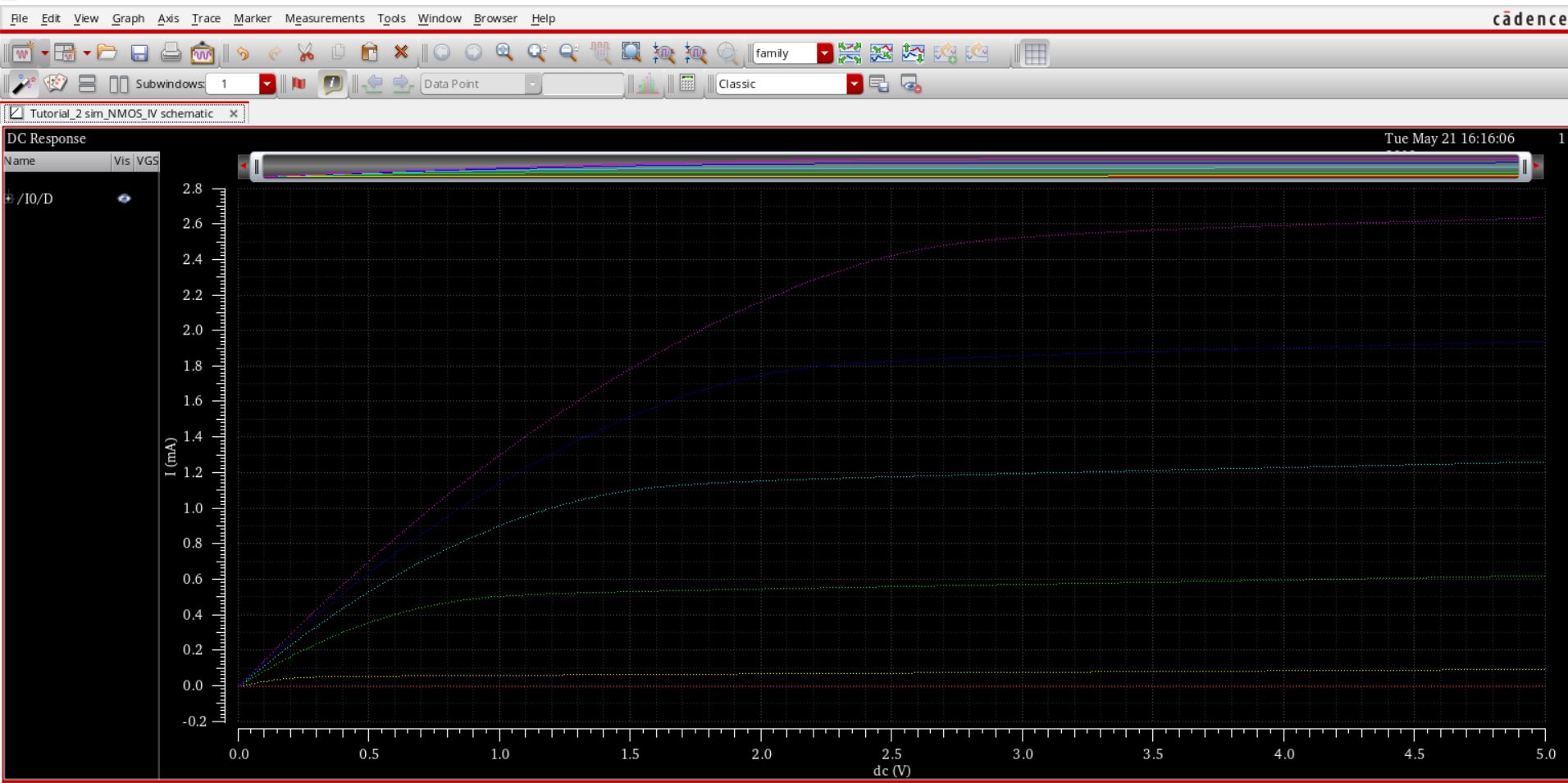
As we see we get the same plot. Do not
save the current state when
exiting.
PMOS
We are going to repeat most of the same steps that we did for the NMOS.
Now that we know what we are doing we will go a little faster.
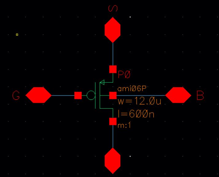
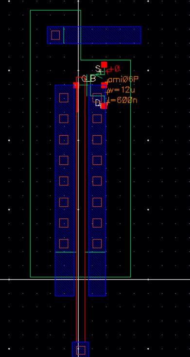
Create a new schematic cell called PMOS_IV. It will have a W of
12u and a L 600n. The pins are inputOutput. Below is an example. Check
and save when finished.
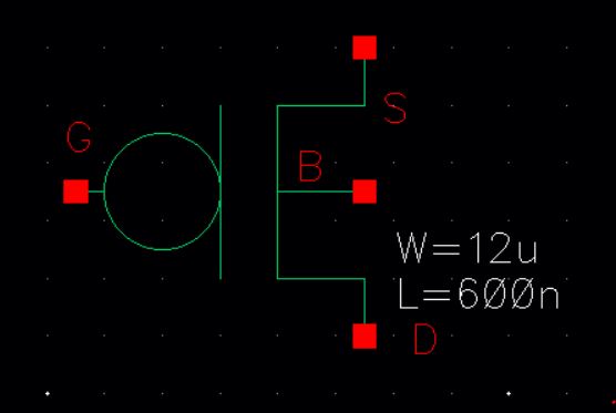
Now create a symbol for the schematic. For assistance look back to NMOS
and Tutorial_1
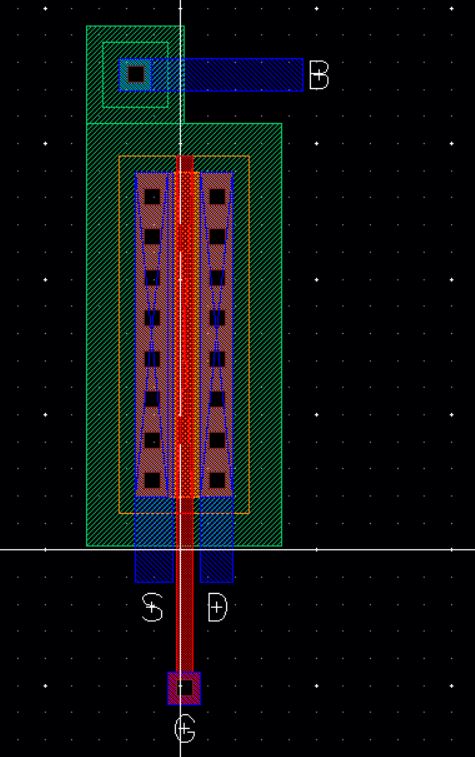
Next create a Layout. You will need pmos, ntap, and m1_poly.
Remember to change with width of the pmos. Add pins, metal1,and poly.
Save and DRC. Fix errors that appear.
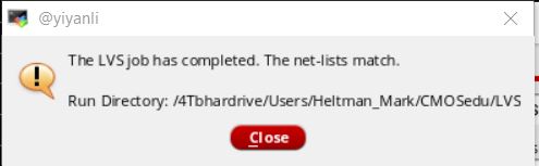
Now extract the layout, open it and run a LVS.
Click "Ok" if asked to save
If the LVS runs without error continue with the simulation
portion.
Close and save all open views.
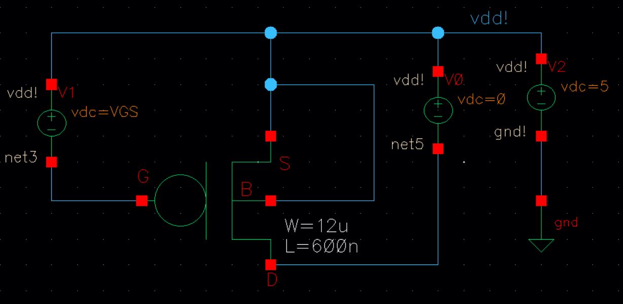
Create a new schematic cell called sim_PMOS_IV.
In the schematic create the following circuit.
We are now ready to simulate open ADE L.
Set the simulation to spectre.
We need to set up a
model for spectre to use, mouse over to "Setup" then to "Model
Libraries" .In the new
window double
click on "models" then "spectre "then to "standalone". Once in
"standalone" select ami06P.m and press open.
The Analyses will be set as
before and for reference you can see it below.
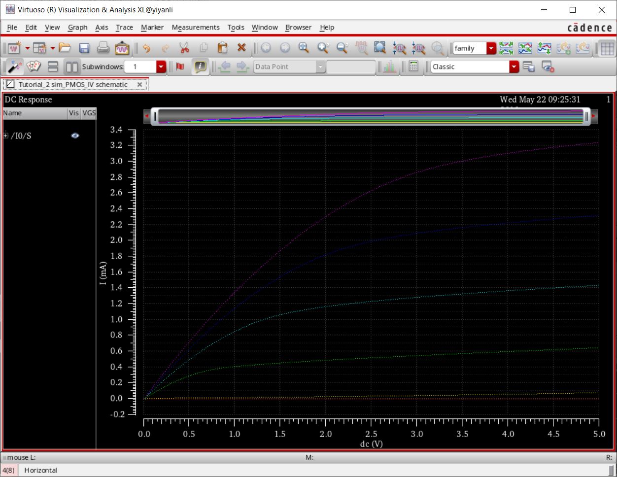
The output we will save and plot is pin "S"
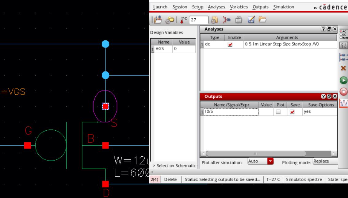
Now mouse over to "Tools" and set up the parametric analysis.
The plot should look like this.
Now run the simulation using the extracted view. Like shown previously.
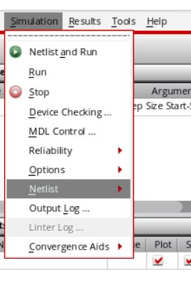
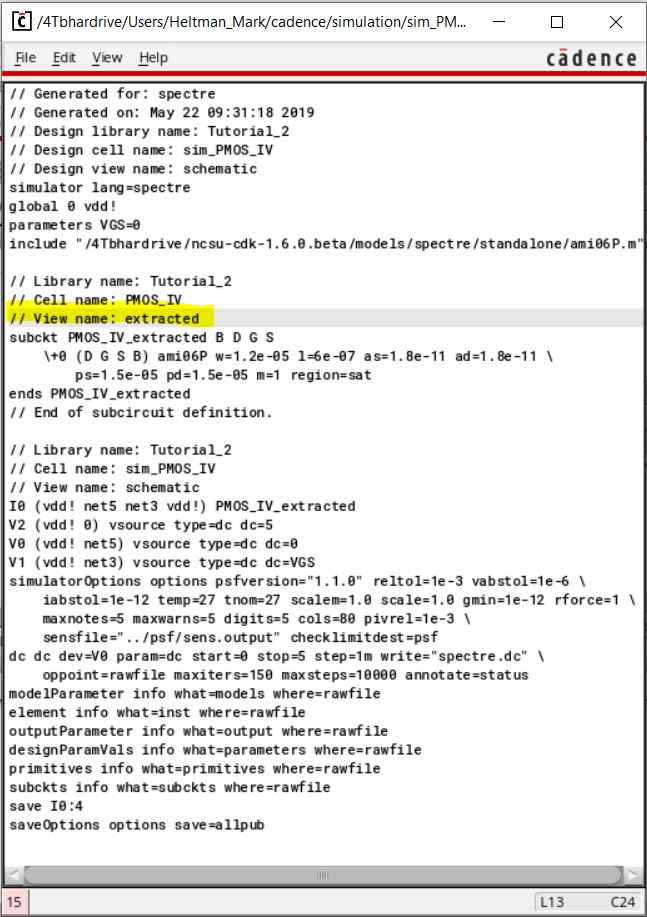
To check that the simulation ran from the extracted view go to
"Simulations" then to "Netlist" then click on "Display". In the window
that pop up, look for the view name to be extracted. After
changing the Environment options do
not save the state.
Congratulations you have finished the second tutorial!!!!!.