Tutorial 1: Initial set up and Voltage Divider.
Start MobaXterm
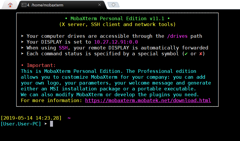
This is your
command terminal which is used to
access the Cadence server
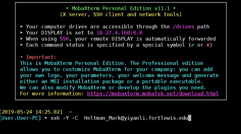
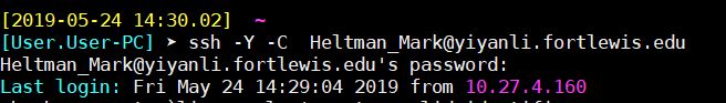
To connect to
the server type in the command window
"ssh -Y -C <your_assined_name>@yiyanli.fortlewis.edu" and then
press enter(
see sample below)
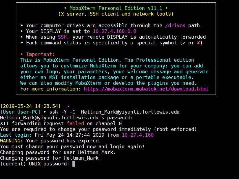
You will now
be asked to type in your temporary
password. When you are typing in your password nothing will display on
the screen.
The following
will appear:
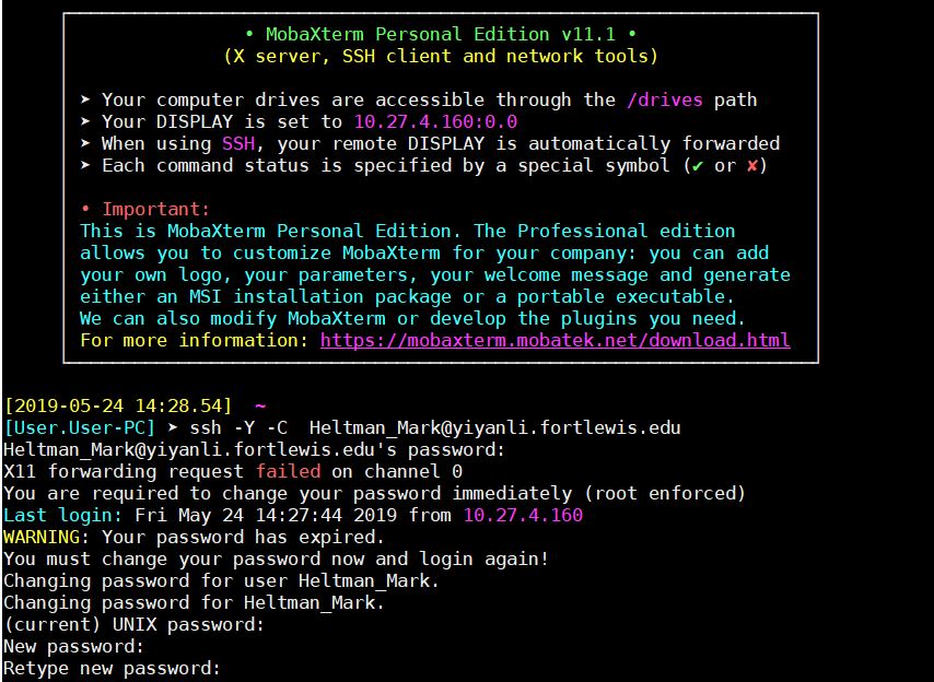
Retype your
temporary password to get the following
couple of lines. Nothing will display as you are typing your
password.
Now Type in
your new password it must meet these
requirements:
- minimum
length = 8 characters
- at
least one uppercase letter
- at
least one digit
- at
least one special character
This ensures that the
terminal will not freak-out at you and that your
account is secure.
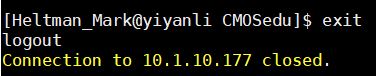
When done correctly your
connection will be closed

To re-login type in the
terminal window "ssh -Y -C
<your_assined_name>@yiyanli.fortlewis.edu" and press enter. Or
recall the
previous command by pressing up arrow and then enter.
Type in your new password and
the following will appear:
Now, in the command window
type in "clear" then enter to clear the
command window.
Using the
Command Window
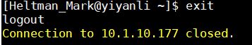
WHEN ITS TIME LOGOUT TYPE IN
THE COMMAND WINDOW "EXIT" THEN PRESS ENTER IF THAT DOES NOT WORK, IN
THE COMMAND WINDOW PRESS "CTRL AND C"
In
the terminal you will need to know a few commands now that initial set
up
is done.
To run a command type in the
command in and then press "enter" or "return"
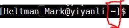
This place is called your
home directory. This is where you
will navigate from to setup and start Cadence.
The "~" will change to
indicate your current directory. "~" is your
home directory. Directories are case sensitive.
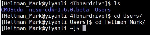
Now the directory is
Users.
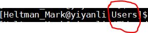
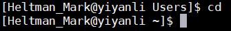
The "cd" command will take
you from any directory and return you back
to your home directory.
Below the cd command is
taking me from Users back to my home directory ~
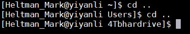
To move up a directory type
"cd .." then press enter
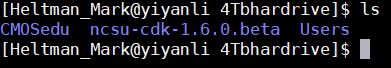
To view directories that you
are able to move down into type in the
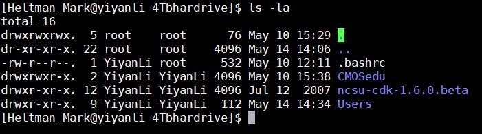
command window "ls", to view everything in a directory including hidden
files type "ls -la"
To move down a
directory type cd
<namedirecotry> and press enter.
In the
sequence below I use the "ls" command to
see which directories I can move to. Then I type "cd Users"
to move down the Users directory.
Finally I type
" cd <username>" and low and
behold I'm back to my home directory
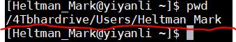
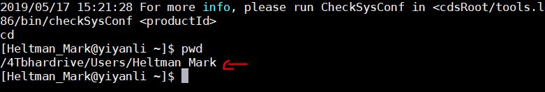
"pwd" is a
very useful function. When typed
into the terminal it displays the entire path to your location. This is
the absolute path to my home directory (underlined in red).
To get help on
any command type " <command>
--help". Using "cp --help" , where "cp" is the is the copy command we
get:
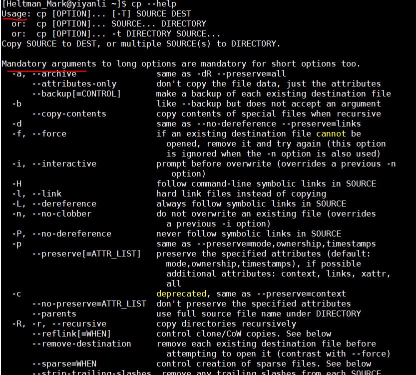
In most cases
it will tell you the usage of the
command and all of the arguments that can be used with the command
(underlined in red)
Getting Cadence and Virtuoso started.
1.)
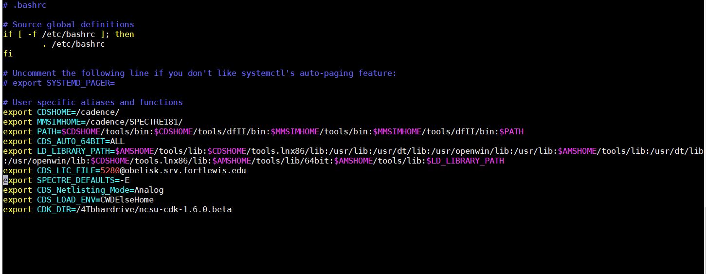
Edit the .bashrc file
Navigate to
your home directory.
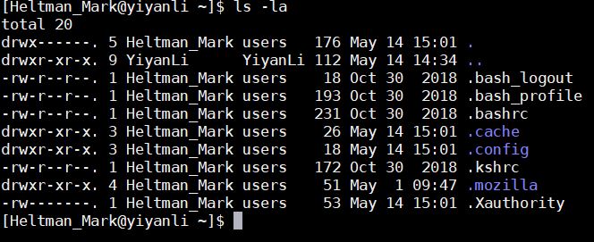
.bashrc is a
hidden
file. To see it type "ls -la" in to the command window.
To edit, type
into the command window
"vi .bashrc" or "nano .bashrc" or use your
favorite txt editor.
Add the
following to the .bashrc file.
export CDSHOME=/cadence/
export MMSIMHOME=/cadence/SPECTRE181/
export PATH=$CDSHOME/tools/bin:$CDSHOME/tools/dfII/bin:$MMSIMHOME/tools/bin:$MMSIMHOME/tools/dfII/bin:$PATH
export CDS_AUTO_64BIT=ALL
export
LD_LIBRARY_PATH=$AMSHOME/tools/lib:$CDSHOME/tools.lnx86/lib:/usr/lib:/usr/dt/lib:/usr/openwin/lib:
/usr/lib:$AMSHOME/tools/lib:/usr/dt/lib:/usr/openwin/lib:$CDSHOME/tools.lnx86/lib:$AMSHOME/tools/lib/
64bit:$AMSHOME/tools/lib:$LD_LIBRARY_PATH
export CDS_LIC_FILE=5280@obelisk.srv.fortlewis.edu
export SPECTRE_DEFAULTS=-E
export CDS_Netlisting_Mode=Analog
export CDS_LOAD_ENV=CWDElseHome
export CDK_DIR=/4Tbhardrive/ncsu-cdk-1.6.0.beta
The final
file should look like this:
Save then
quit the .bashrc file.
To re-initialize
the file type ". .bashrc" into the command window
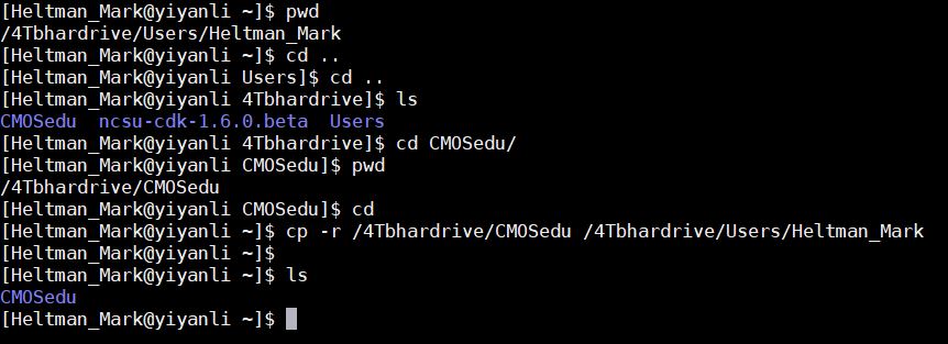
We will now
copy over CMOSedu to your home
directory.
Copy it over to
your home directory using the command "cp -r
/4Tbhardrive/CMOSedu <Your home direcotry> "
(where r means recursive)
To determine
your home directory use the "pwd"
command. Below is how to determine everything from scratch using only
the
commands we know how to do. The last "ls" is to see if
there is a CMOSedu directory in our home directory.
Navigate
into to the CMOSedu
that is now in your home directory.
Add the following
lines to cds.lib file using your favorite txt editor.
DEFINE analogLib
/cadence/tools.lnx86/dfII/etc/cdslib/artist/analogLib
DEFINE functional
/cadence/tools.lnx86/dfII/etc/cdslib/artist/functional
DEFINE sbaLib
/cadence/tools.lnx86/dfII/etc/cdslib/artist/sbaLib
The finished
file should look like this:
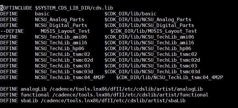
The cds.lib
are where the cadence libraries are
defined.
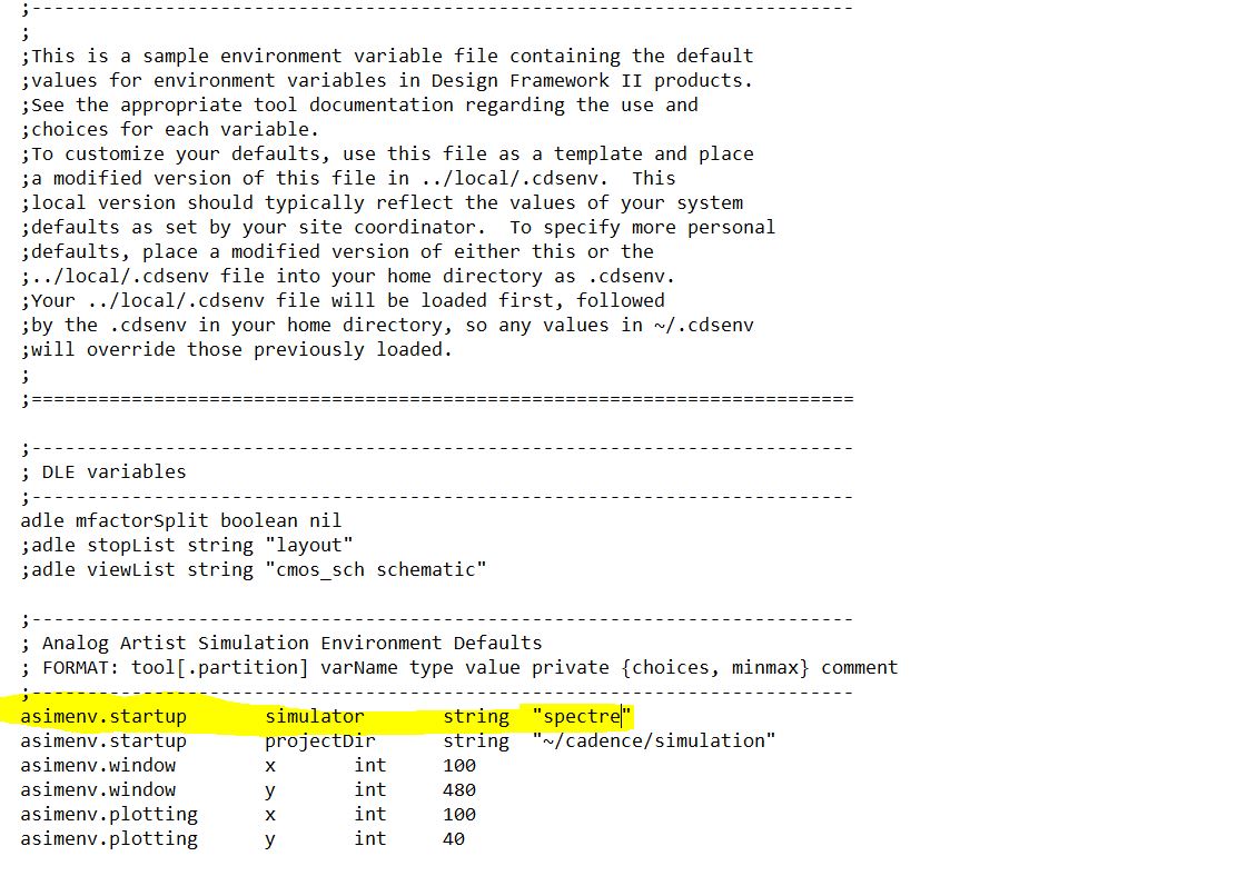
Set the simulator default to "spectre" open the .cdsenv file. Then change the simulator from "hspiceD" to "spectre".
HOW TO START
To start
Virtuoso navigate to the CMOSedu and type
"virtuoso
&" in the command window
"&" will
allow you to still use the command
window.
If you get an
error:

Then navigate
back to your home directory and type
". .bashrc" into the command window, Then navigate back to CMOSedu and
type "virtuoso &"
TO
LOGOUT, CLOSE CANDENCE THEN,TYPE IN THE COMMAND WINDOW "EXIT" THEN
PRESS ENTER
Voltage
Divider Tutorial1
Log
on to the Cadence server by navigating to CMOSedu and typing "virtuoso
&" into the command window.

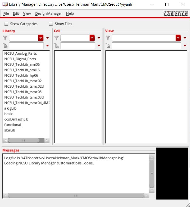
Two windows
will appear on your screen. In order they are the Command
Interpreter Window and the Library Manager. The Command
Interpreter Window (CIW) is where commands, reports,
and errors will be printed. The Library Manager is where all of
your saved instances can be found.
( The windows have been resized for the tutorial)
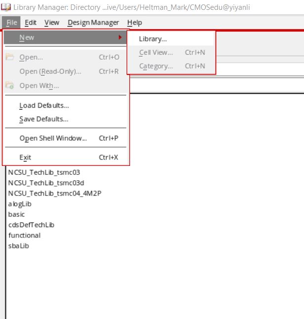
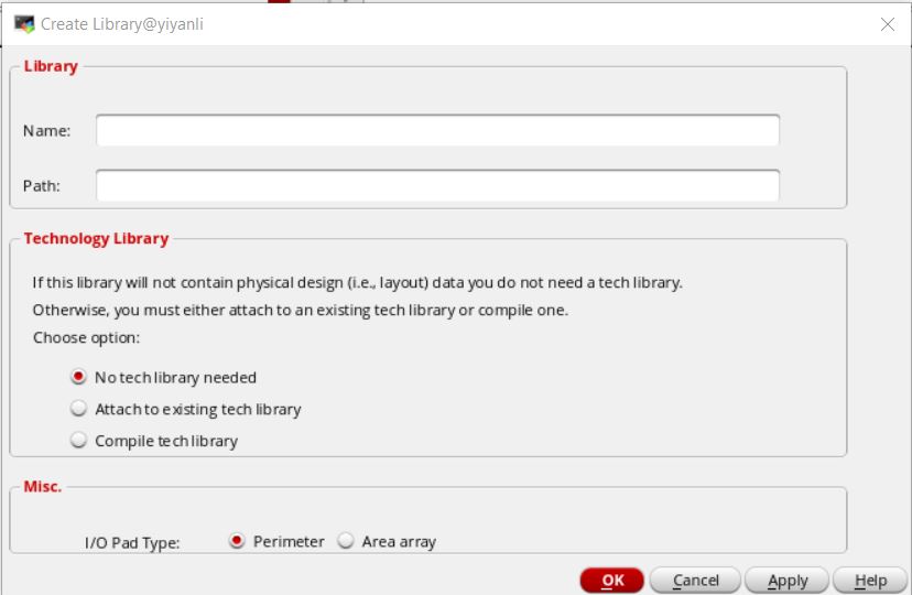
In the Library Manager mouse
over to "file" then to "New" and click on "Library"
Open MobaXterm and navigate
back your home directory and use the pwd command. This will be the save
path for the new library.
In the " Create Library"
window
pick a name for tutorial 1 ( names cannot have spaces in them),
for the path put down the path that was found using the pwd
command.
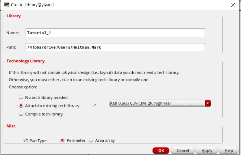
Change the technology Library
to "attach to existing tech library" and pick the library used by
the professor. I used AMI 0.60u. Then press ok.
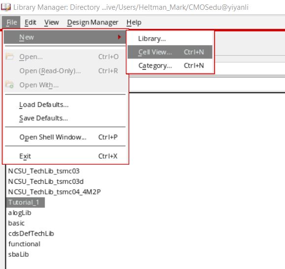
You can now see that the tutorial has been added to the list of
libraries.
Click on
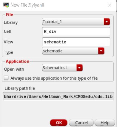
Tutorial_1 then go to "file" then to "New" then to "Cell View". This is
how we will creating the most of the cells that we need.
We will call
the cell "R_div". Make sure that view is schematic and the type is also
schematic, and click ok.
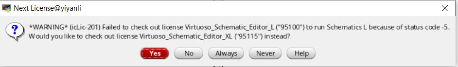
A warning
window will pop up, in it click "Always".
The next
window will be where we will be placing down components to build the
voltage divider.
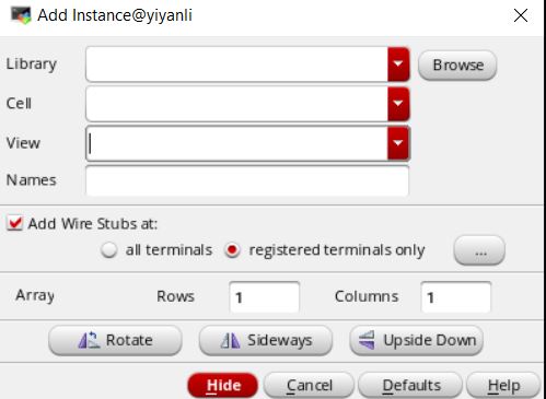
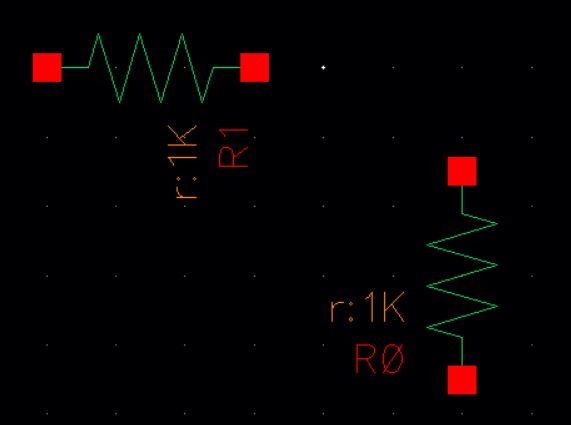
To start
laying down components press "i" or click on  button.
In the window
that pops up use the drop down menu to change the Library to
"NCSU_Analog_Parts". In cell type "res" to get a resistor.
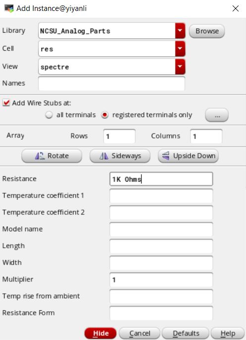
Press Hide to
start placing down your resistors, Left click to place and right
click to rotate. Use the mouse wheel to zoom in and out, press in
the mouse wheel to drag the work space. Press "f" to
automatically resize the window.
Press"ESC" to
cancel. To undo press "u"
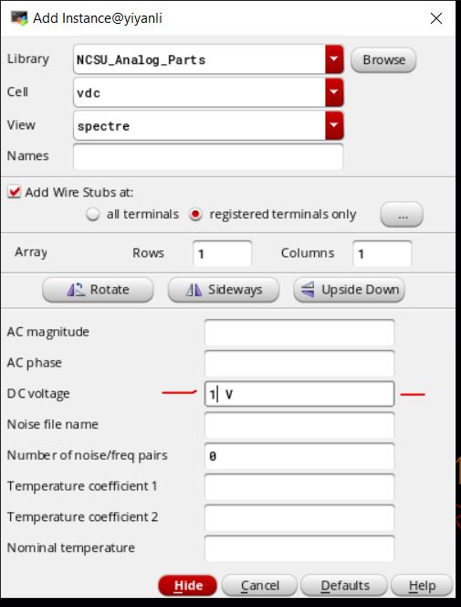
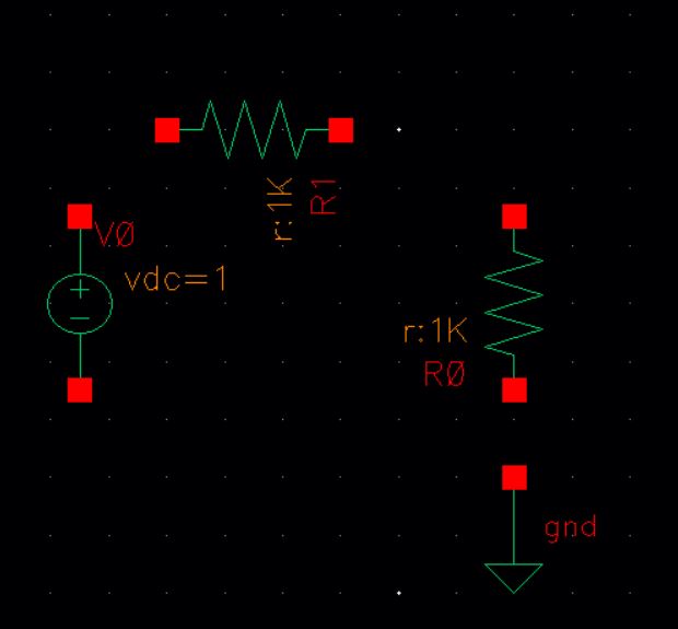
Now we will
need a voltage source press "i" to bring up the " Add instance" window
change the cell to "vdc" (voltage dc source)
Set the DC
voltage to 1. (where the red lines are). If the lower part of the
window does not appear click below the " Rotate button"
Click hide and
place down the voltage source. Press after placing the
voltage source press and "ESC" then press "i' and change
the cell the gnd for ground the view will change symbol.
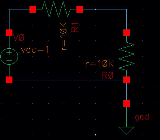
The final
circuit should look like something like this:
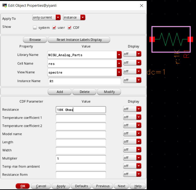
To change the
options for a component, click on the component and press "q".
Change the resistance to 10 K ohms and press ok. Change the other
resistor to 10 K Ohms as well.
To wire
components together press "w" or click on  . The
completed circuit should look as follows.
. The
completed circuit should look as follows.
Onced wired
click on " Check and save"  return to
the CIW and double check that there are no errors.
return to
the CIW and double check that there are no errors.
To label
wires to the schematic click on  which
will bring up the wire label menu.
which
will bring up the wire label menu.
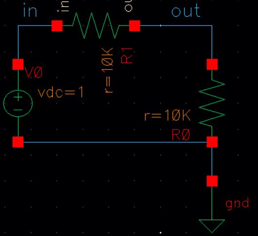
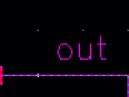
Name the wire
"in" then press hide and click on wire leading into the R1
resistor. Name another wire "out" and put it on the output of
the R1 resistor. Click on check and save when finished.
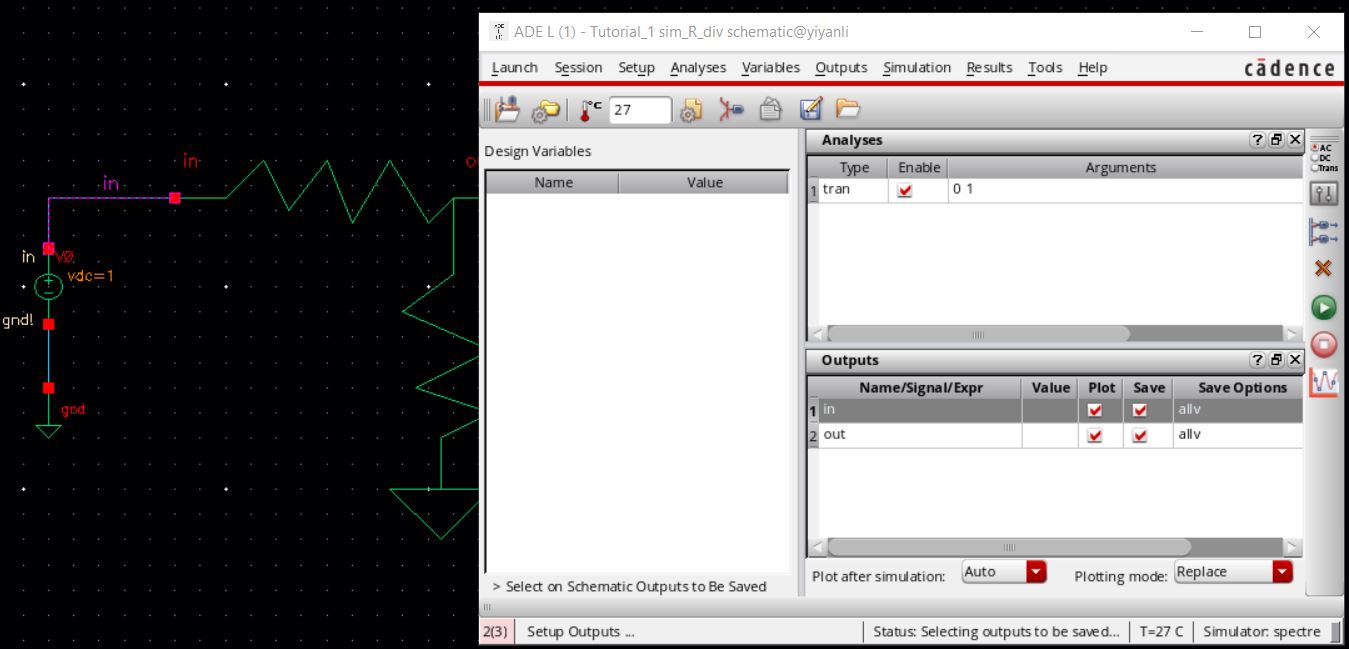
We are now
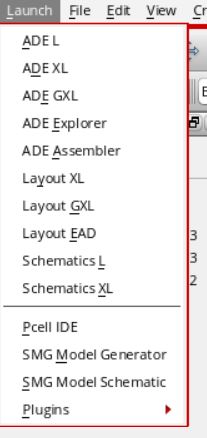
going to launch the simulation software. Mouse over to "Launch" and
click on "ADE L" .
A pop up
window will appear click on always.
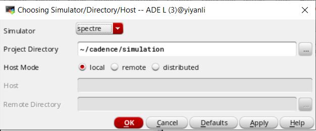
To confirm that simulator is
"spectre" mouse over to Setup then click on Simulator/,,,,
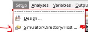
In the popup window confirm that the simulator is "sptectre".
Then press "ok".
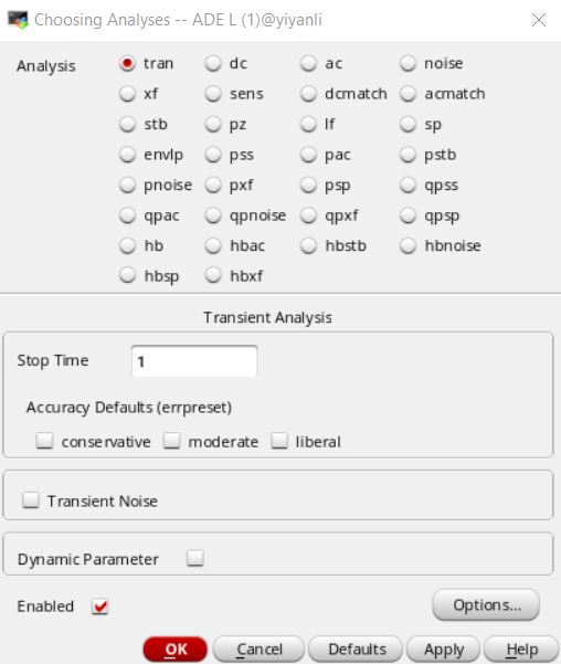
To set up the type of
analyses, mouse over to Analyses and click on "Choose". In the popup
window set "Analysis to "tran" with a stop time of 1 (units are in
seconds), click enable. Press "ok"
To plot save and plot
signals click on "Outputs" then click on " To Be Saved" then
"Select on Design"

Go back to schematic and
click on the wire labeled "in" and the wire labeled "out".
When a wire is selected, the wire and the wire name will turn a
different color.
In the Outputs window click
the plotted boxes. The final ADE window will look like this
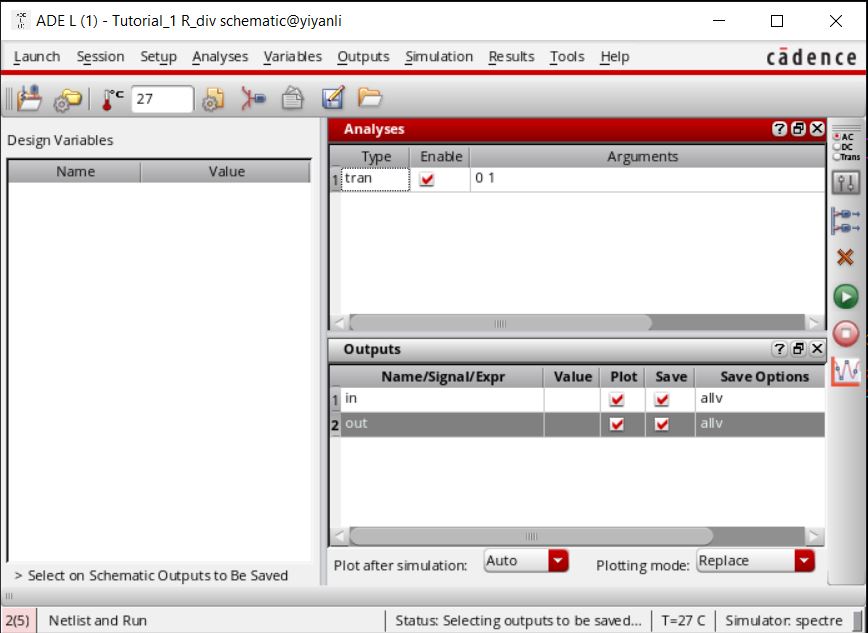
Once everything is set up click run  .
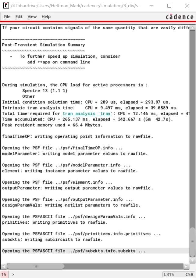
Once the simulation is complete two new windows will pop up. The first,
is a log of everything that happened, it will contain information about
CPU usage and time to run the simulation. This window is only
needed if there are errors while running your simulation.
.
Once the simulation is complete two new windows will pop up. The first,
is a log of everything that happened, it will contain information about
CPU usage and time to run the simulation. This window is only
needed if there are errors while running your simulation.
The other view is the plot
with our inputs and outputs. Our input should be at 1V and because this
is a voltage divider our output will be at .5V.

Close out of the
plot.
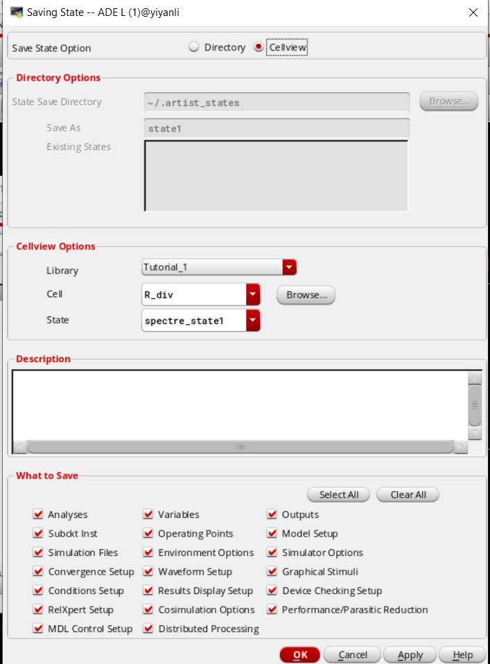
This was just a test to view and learn the analysis tool. save
the set up by clicking
on "Sessions" and "Save State"
In the new window set the
save state option to "cell view", Then press "ok". Once the view has
been saved close the ADE window.
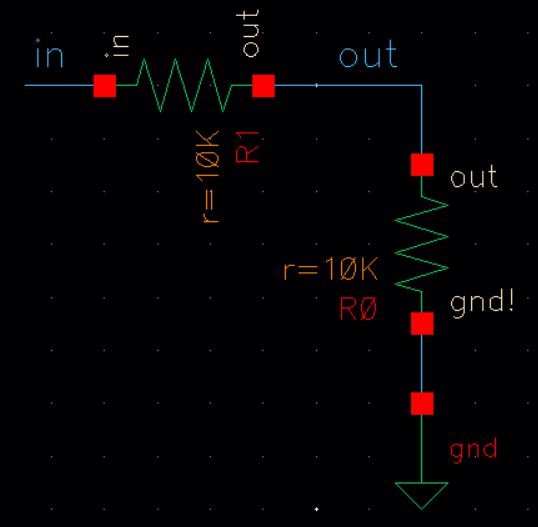
Return to the schematic and
delete the voltage source and the wires connecting it. The
schematic should look as follows.
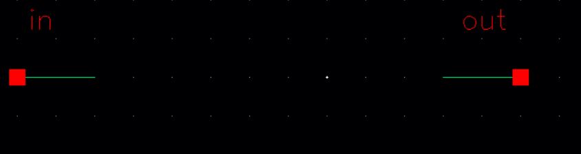
To add pins to schematic press "p" or  button. Name the first pin "in" and make sure the Direction is
set to "input". Press hide and place the "in" pin on the "in"wire
Name the second pin "out" and make sure the direction is set to
"output".
button. Name the first pin "in" and make sure the Direction is
set to "input". Press hide and place the "in" pin on the "in"wire
Name the second pin "out" and make sure the direction is set to
"output".
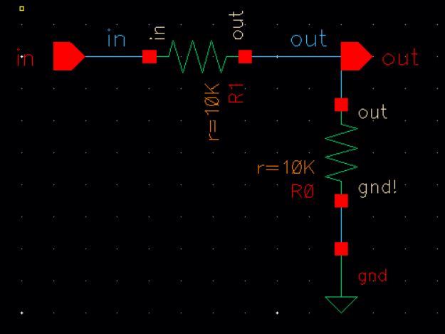
After the schematic should look like as follows. When finished
click on "check and save". There should be no errors reported in the
CIW.
We are now going to create a symbolic view of this design. To begin,
click on "Create" then to "Cell view" then "From Cell
view".

In the pop up window make sure that the view name is "symbol". Then
press "ok".
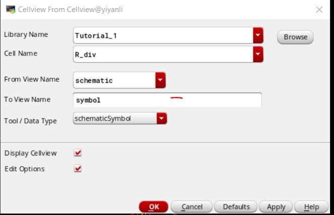
In the next pop up window press "ok"
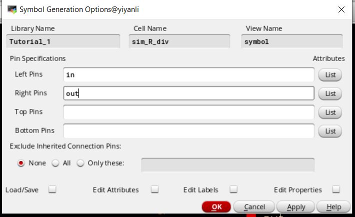
The view that is generated by automatically by the Symbol tool is not
really help full. We will draw our own symbol for the schematic that we
just created.
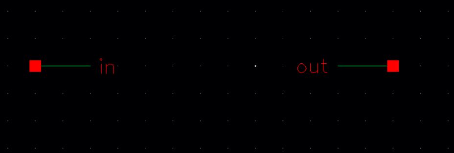
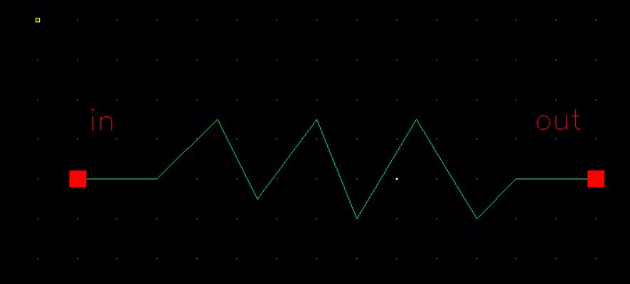
To do this, delete everything but the pins. When finished it should
look
as follows.
To move the labels out of the way press "m" and then click and
move the label. Click and dragging does not work. Press "ESC" to
close out of the current tool.
Now click on "Create" then to
"Shape" then to "Line". A new window will pop up, click on "Hide". To
draw, click on where you want to start then click on the next point and
a line will be drawn. To stop drawing double click on the point
where you want to stop,
The first resistor should look something like below.
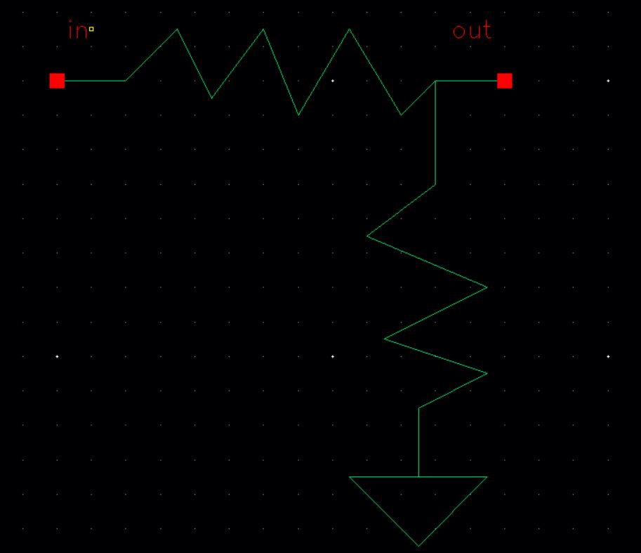
Once the first one has been drawn, draw the second resistor and a
ground symbol. The final drawing should look something like as
follows. When you are finished Check and Save the
Symbol.
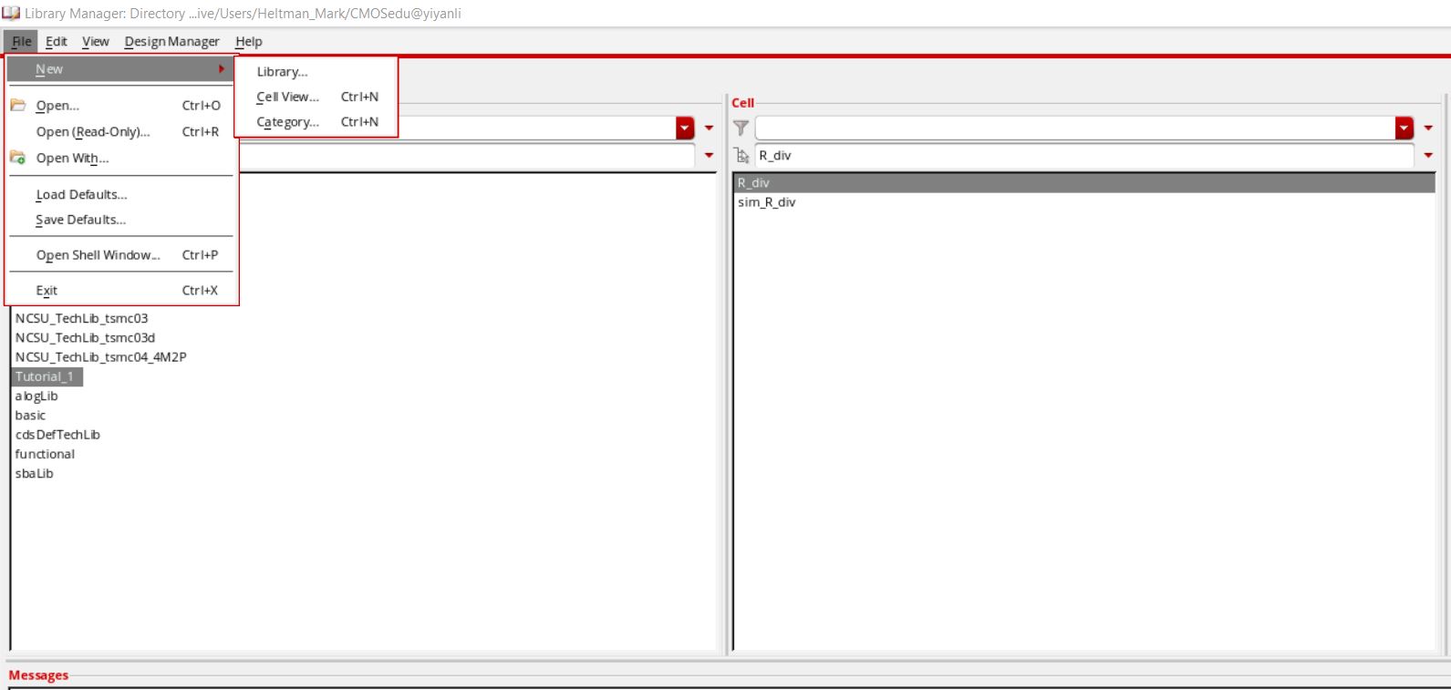
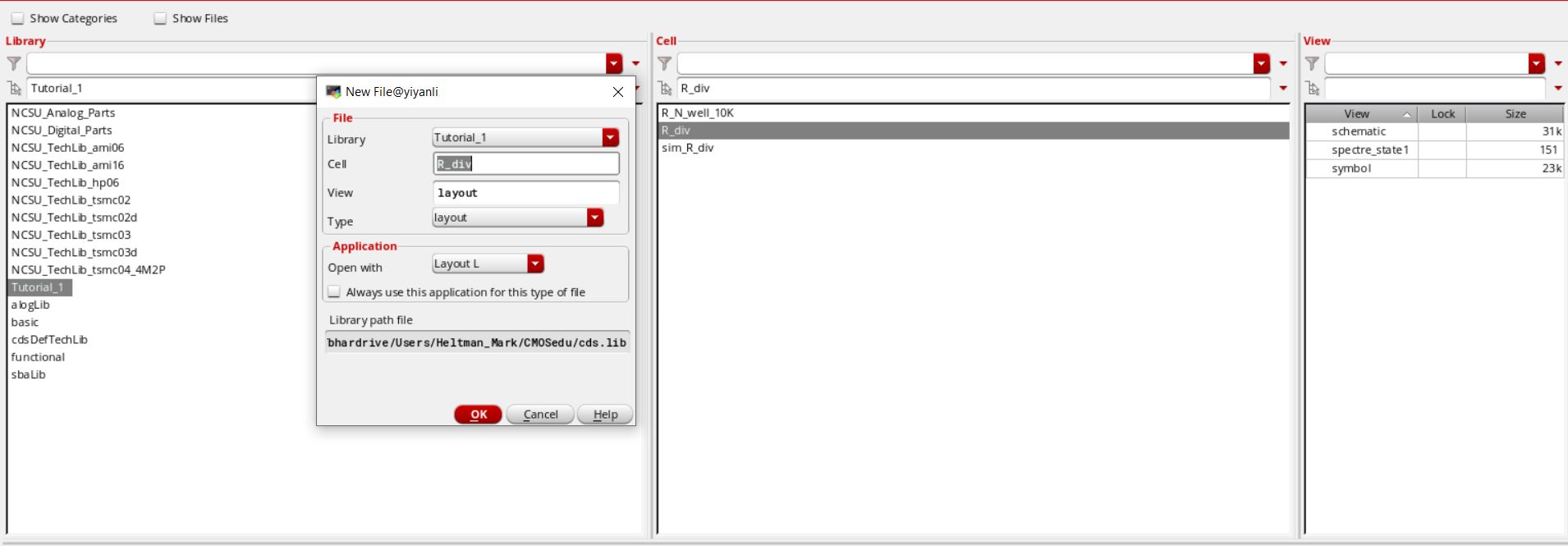
Now we are going to create a simulation library where only the files
necessary to the simulation live.
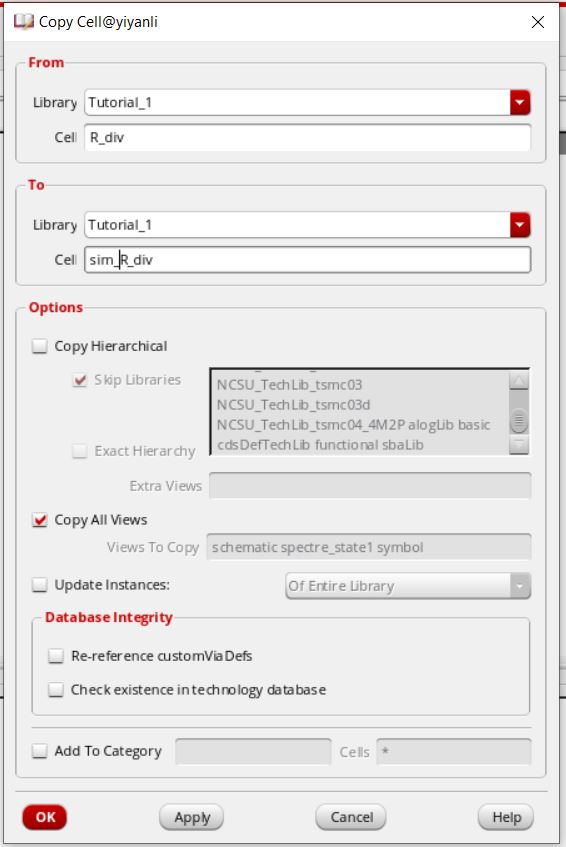
Close out of both the symbol view and the schematic view. In the
Library Manager, right click on the R_div and then click "Copy". In the
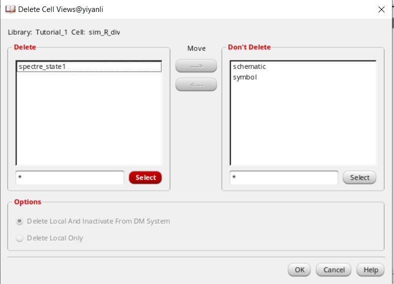
copy window change the two cell to "sim_R_div", Then press "ok".
Now delete "spectre_state1" and "symbol". To do this right click on the
View and click on "Delete". In the pop up window make sure that
everything is correct then press "ok",then "yes"
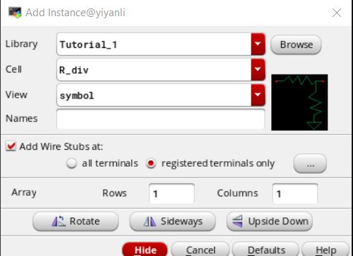
Now open the schematic view in sim_R_div and delete everything in
it. We are going to replace it with the symbol that we just
drew. Press "i" and bring up the component selector. Change the
Library to " Tutorial_1"
Change the cell to "R_div". Press "Hide" and place the symbol in the
schematic.
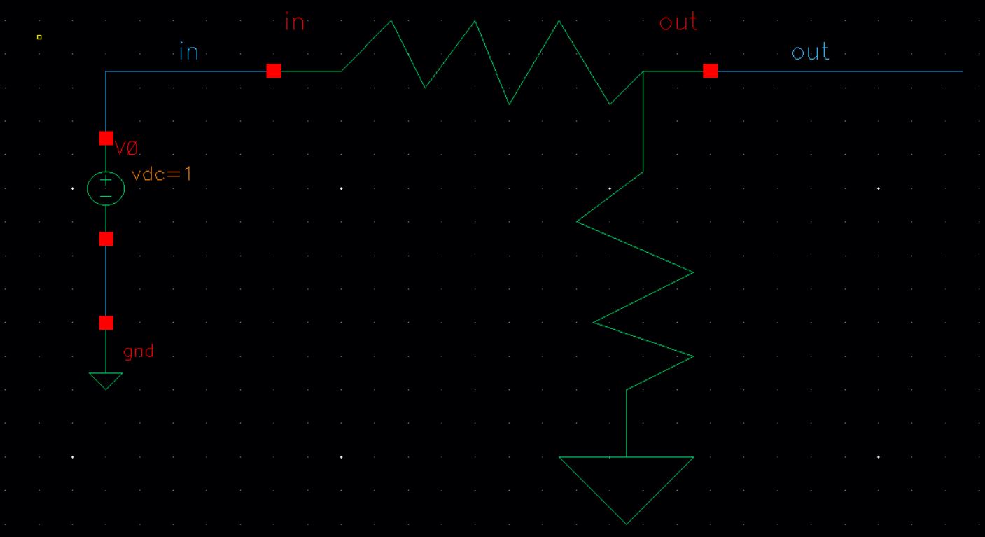
Add a power source, ground, and wires. The power
source
is 1V. All of the parts are found in the NCSU_Analog_Parts.
When you are done it should look like this:
Check and save. Note there are warnings. To view the warnings
mouse over to "Check" then to "Find Marker". We will figure out
the errors here.
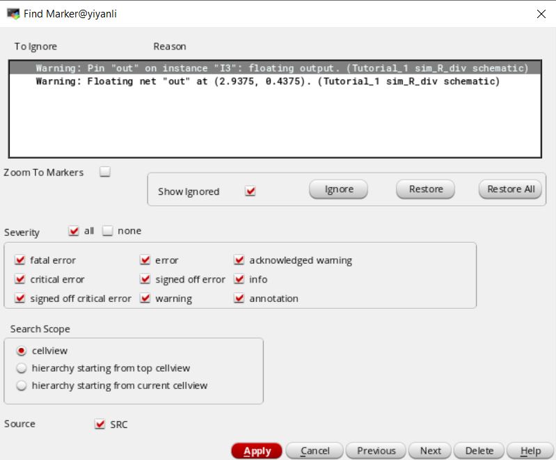
To zoom to an error check the "Zoom To Markers" box then click on the
error you wish to view. The errors that are on the
"out" pin and on the "out" wire are because they are floating, meaning
they are not connected to anything. In our case we can
ignore
the errors. To do this click on the ignore button and a start(*) will
appear next to the ignored errors. When the errors have
been ignored click "Apply" then close the window. Then run another
check and save. Now there are no errors.
Now re-analysis the circuit. Using the same procedure as before
open
ADE L and set it up to run the same simulation as before.
As we can see in the plot, the output voltage is .5V, so nothing
has changed. Save the state by going to "Session" then to "Save
State". Change the box to cell view and save it under sim_R_div.
Before we move on let us see how we can descend through the hierarchy
in
the drawing. In the sim_R_div schematic click on the voltage
divider symbol. While it is selected mouse over to "Edit" then to
"Hierarchy" then to " Descend Edit"
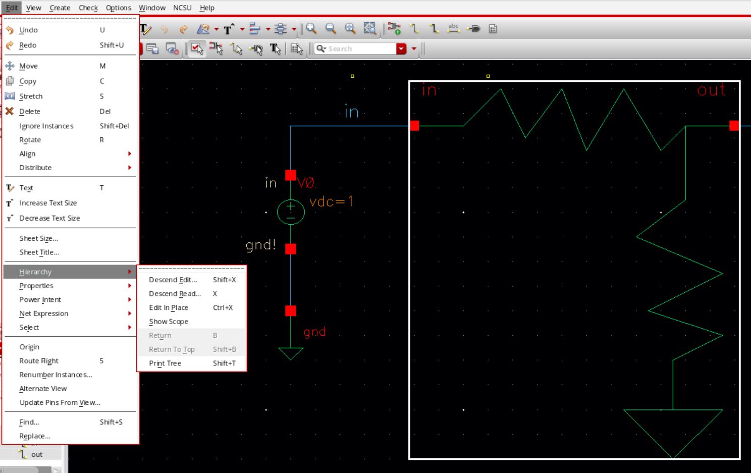
After its been click a pop up window will appear, here you can pick
where you want the view to be. For simplicity, change the bubble
to "new tab" then press "ok".

We now have two tabs. The first tab is the schematic and the
second tab is the schematic that represented by the symbol. This is
very useful you have to make quick edits to the underliying
schematic, or when you need to remind yourself of what is in the
symbol.
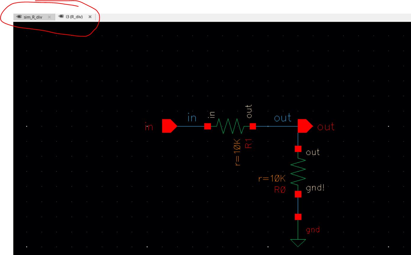
Close out of both of those drawings.
We are now going to layout a resistor.
Return back to the library manager and have Tutproal_1
highlighted.
Mouse over to "File" then "New" then " Cell View".
In the pop up window, call the cell "R_N_well_10K" in the view section
remove "schematic" and type
"layout". The "type" will automatically change. Then press "ok" .
In
the next pop up window click on "Always" just like before.

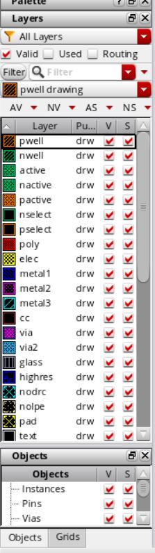
On the left had side we have all the layers that we can use to make
circuits. For the resistor we will use the nwell layer.
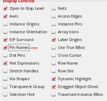
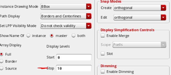
Now mouse over to "Options" then to "Display". In the
Display Options menu we want to set a couple setting that will make our
live easier. First we want to check Pin Names under Display
Controls, Then we want to change our display level from 0 to
10. To save these as our defaults forever click on "file" then
press "Save To". Then press ok to leave the settings.
Make sure the nwell layer is selected and then press "r" this will
allow you to draw a rectangle. Press hide on the pop up menue.
Draw one rectangle of any size.
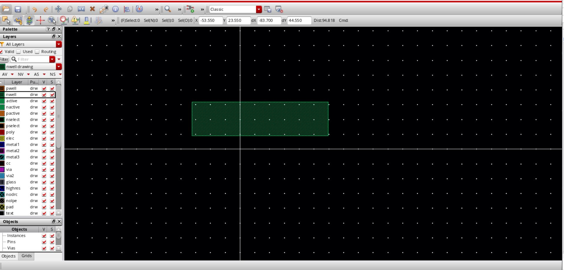
We want resistor that
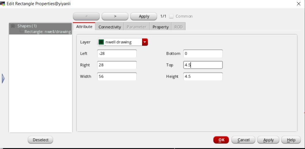
is 56 um long and 4.5 um wide. Click on one of the green boxes
and press "q" this will allow us to change its properties. Modify
the dimensions so that it is with in these constraints. When you are
done press "ok" For example I changed the dimensions to as
follows.
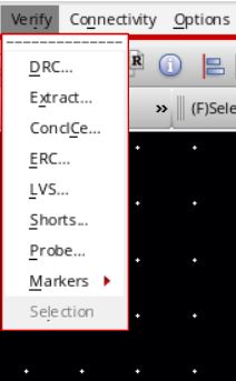
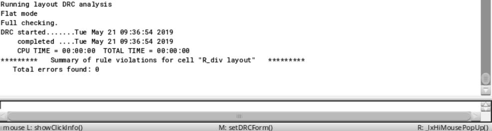
Now we need to check our work. Mouse over to "Verify"
then click on "DRC".
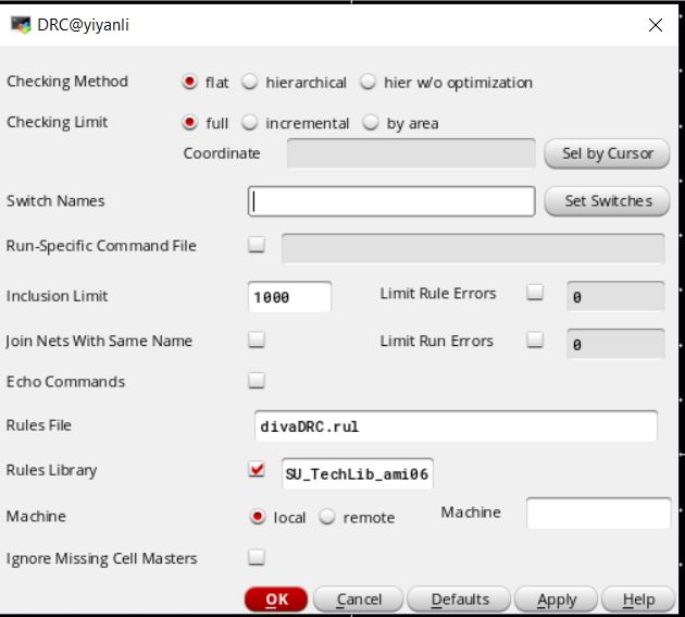
In
the
DRC pop up window press ok to start the DRC analysis.
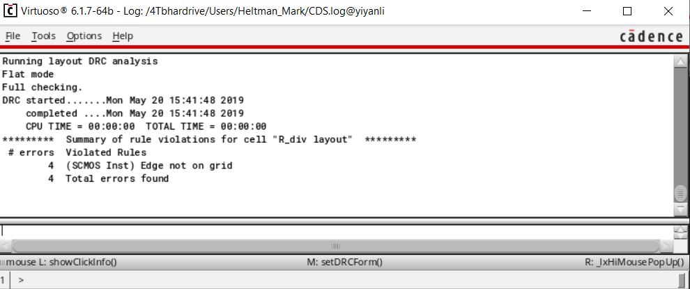
Open the CIW to see how many error and what type of errors they are. In
my case I have 4 errors and they are that my rectangle is not on the
grid. Every layout
you do must pass DRC without any errors.
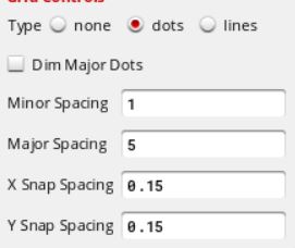
To fix these errors we first need to figure out my grid spacing to do
that mouse over to "Options" then click on "Display". Here we see that
X and Y Snap Spacing is .15. Then close out of the window.
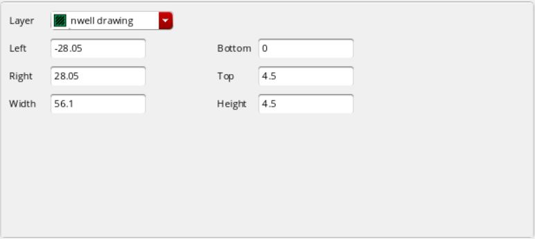
Now we need to adjust the dimensions of the rectangle to fit on this
spacing. The
length of the resistor is 56 and 56/.15 = 373.33 which is not a hole
number so we need to get as close as we can. For
the width we used 4.5 and 4.5/.15 = 30 which is a whole number, so in my cause I had to change mine to
what is seen below.
And now when I run DRC I get no errors. 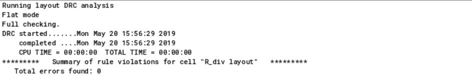
Don't forget so save when needed.
Now we need to add pin connections to the nwell. Press "i" and
change the library to "NCSU_TechLib_ami06" and change the cell to
"ntap".
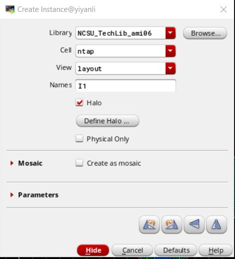
Press hide and place the ntap so that the edge is barley touching the
nwell resistor. 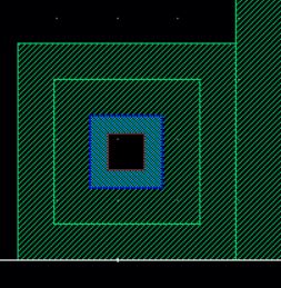
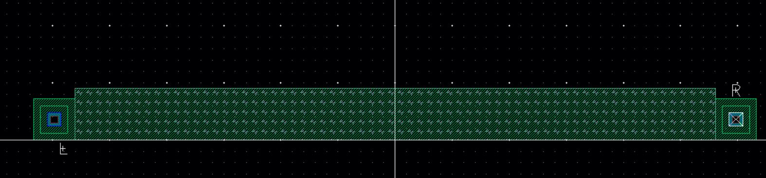
The final resistor should look like the following:
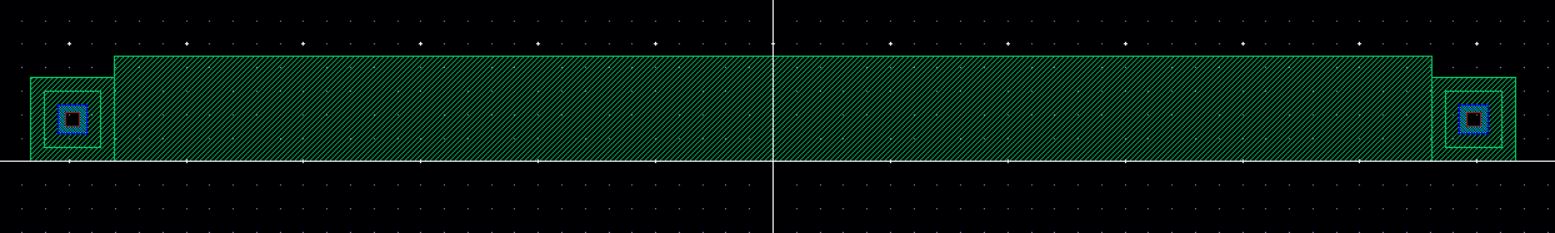
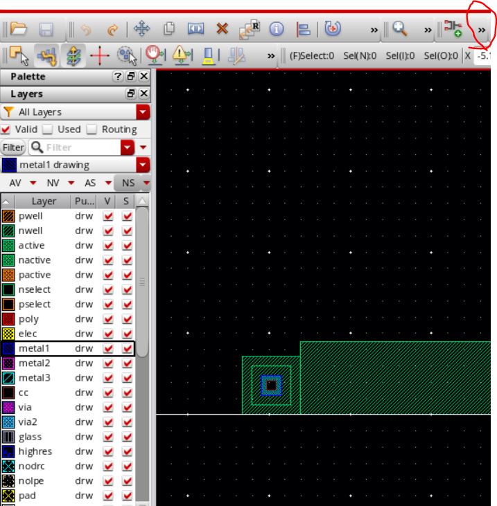
Switch to metal1. Now we will add pins to the Layout. The pins are
found in a dropdown menu next to . See the
red circle in the picture below.
In the create pin menu, the terminal name will be L and check the box
"Create Label".
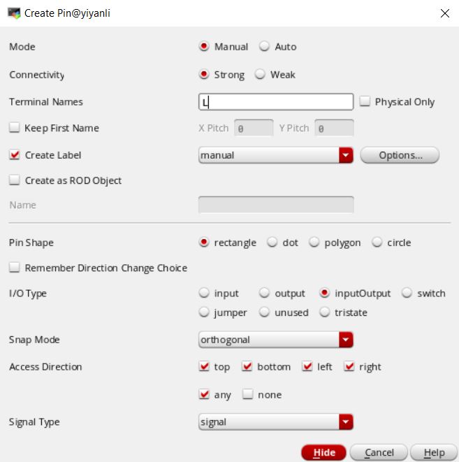
Press hide and draw a box around the blue portion of the left ntap.
Then place the label. The Right side will have the label R. When
this is done mouse over to "Options" then to "Display" and change the
display level stop to 0.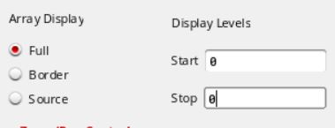 This will show the layer that you
have added. Your completed resistor should look something like
below. When the stop level is 0.
This will show the layer that you
have added. Your completed resistor should look something like
below. When the stop level is 0.

After checking reset the stop level to 10. Now DRC.
There should be one error in the CIW. The computer does not know
that this is a resistor. We have to label it is such. In
the layer selection window scroll down unit you see "res_id"
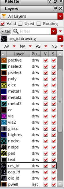
We are now going to draw a rectangle over the resistor that we had
previously drawn. With res_id selected press "r" to draw a
rectangle. You will see little resistor symbols fill in the area
as you draw the rectangle. The finished resistor should look like
this:
Now run a DRC and there should be 0 errors.
To extract the view mouse over to "Verify" then click on
"Extract". In the window that pops up press "ok"
An extracted view is now is your library, open the extracted view from
the library manager.
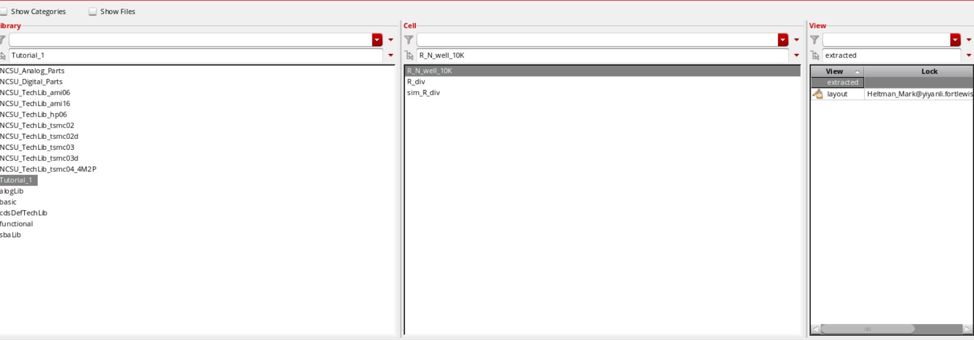
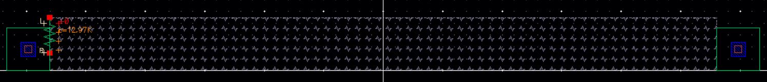
In the extracted view we can see how close we were to creating resistor
that is very close to 10K ohms. We are unable to exactly reach 10K ohms
due to constraints in manufacturing and also because variability in the
nwell layer.
Close the extracted and layout views.
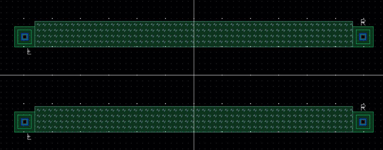
We are now going to build the layout for the voltage divider.
In the R_div cell open a new layout, in the layout place two 10K
nwell resistors. DRC the new layout to ensure there is enough
space in-between the resistors

Should look something like
this:
Now we are going to add metal for the connections. Select metal1
and user to draw the rectangles. Once you are done, DRC the
layout.
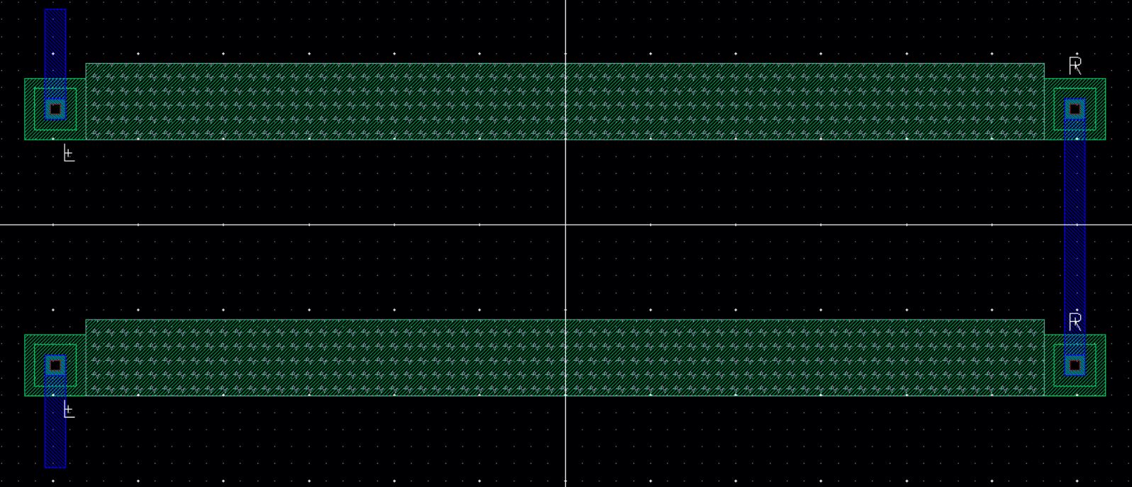
Add pins to the new metal1 layers. They will be named "in", "out"
and "gnd". Use metal1 as the pin metal and make the pin
rectangles the same size as the original metal layers. Make sure
Create Label is checked.
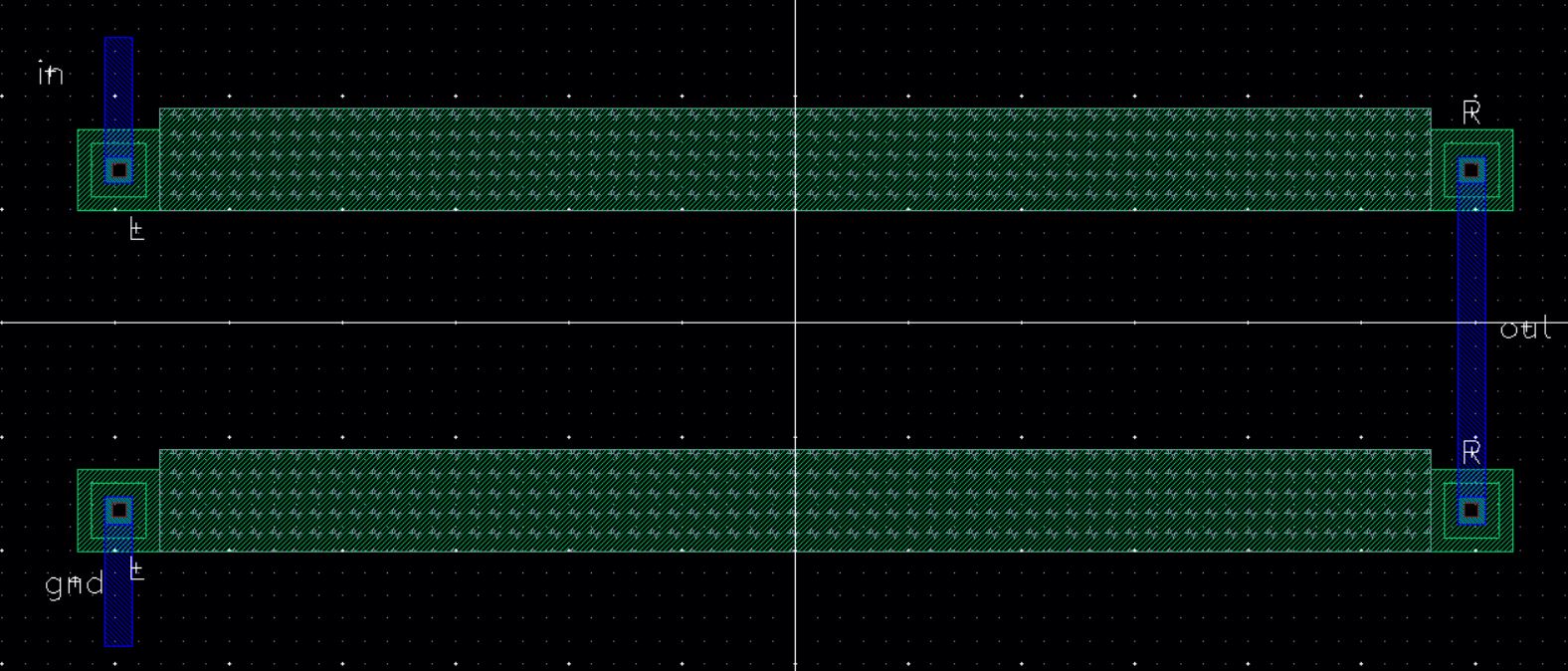
Save, DRC, and Extract your layout.
Now we are going to run an LVS which is layout versus schematic.
Mouse over to "Verify" and click on "LVS"

In the pop up window click on Browse and select the extracted
view that we just created. Then Browse for the original schematic. They
both will be in cell R_div
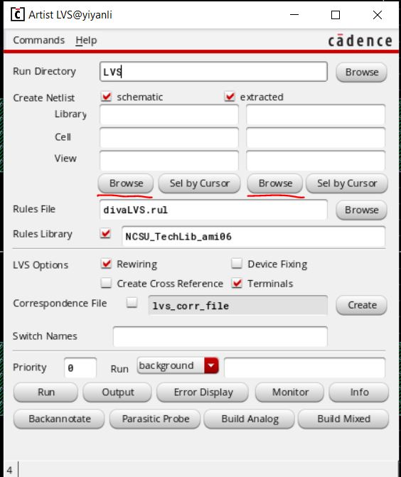
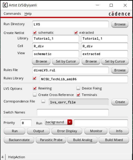
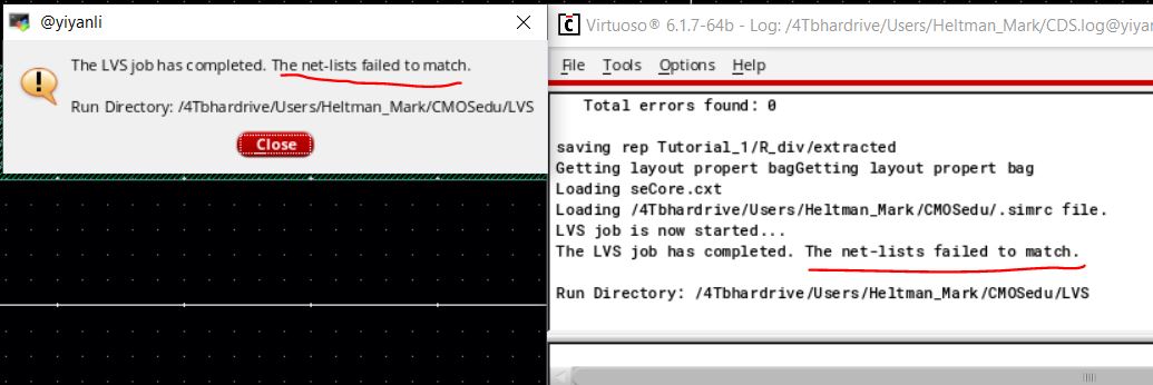
Click on "Run" and the LVS will run it might take a moment. If another
window pops up asking to save press "ok". You can watch it in
the CIW. When the LVS has finished you might see a pop up
window, which will display the results of the LVS. If you do not
get a pop up window, the CIW will also display the results of the LVS.
"The net-lists failed to match" means the LVS failed and the
layout is not the same as the schematic.
To get a more detailed result
of the LVS click on "Output"
From the detailed view we can see that there are 3 main errors.
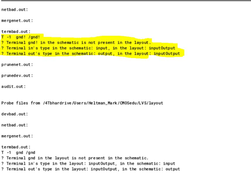
The first one we will tackle is "Terminal gnd! in
the schematic is not present in the layout." In most
layout views we need to have a global ground. Global is indicated
by ! .
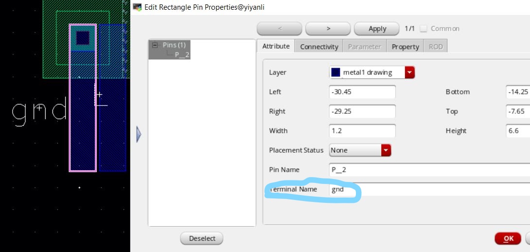
In the layout view click on the gnd pin and press
"q" to bring up the options. You might have to move the
metal1 layer out of the way to get to the pin metal1 layer. Change the
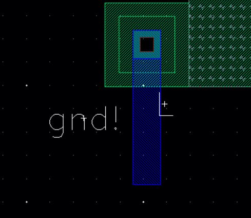
name of the pin from "gnd" to "gnd!"
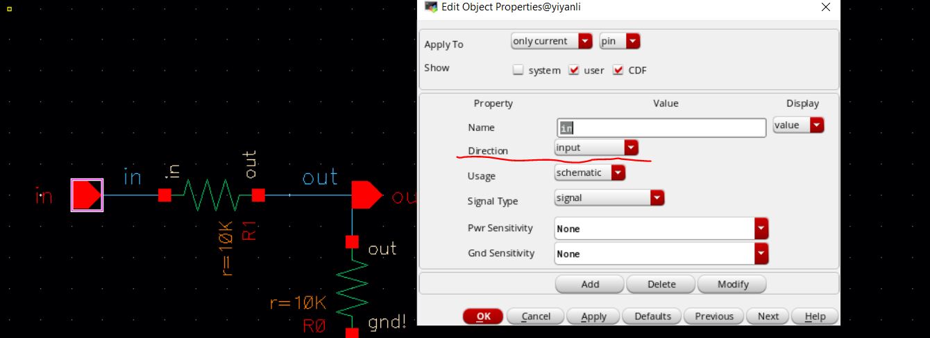
Open the schematic from the R_div cell. Click
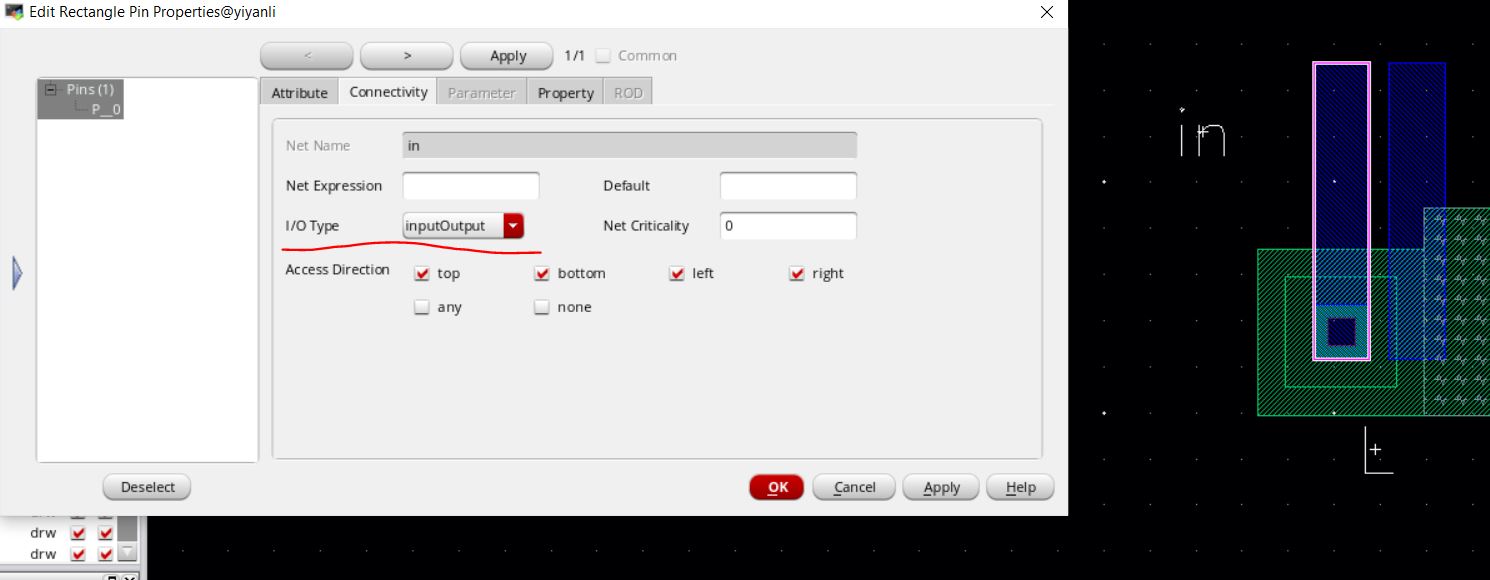
on the pins and press"q" we can see that the direction of the pin is
input. If we return back to the layout we and get the options of
the "in" pin we can see that its direction is input/output.
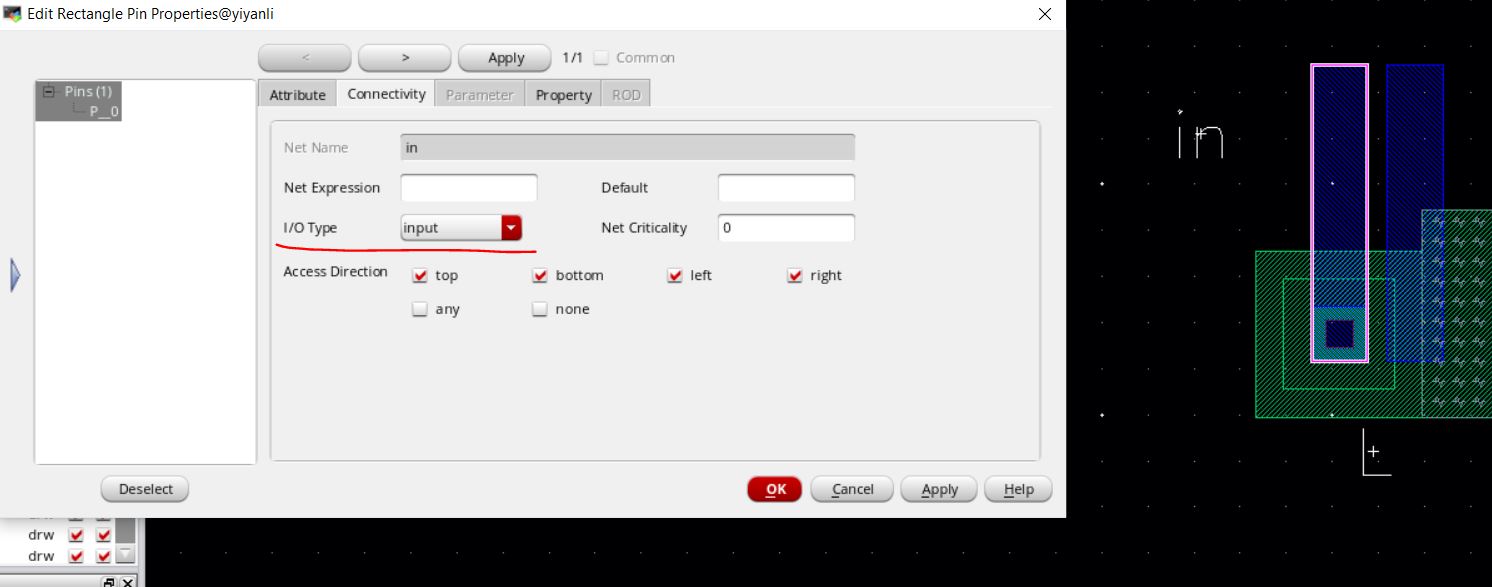
We
need to change the layout pin to input.
We need to do the same thing
on the "out" in the layout, except we need to change it to output to
match the schematic.
When that is done don't
forget to save. Now we need to extract the layout like we had done
earlier. Now run another LVS, this time the netlist should
match. If we look at the click on output we can see that
everything is fine and dandy.
If you still get "netlist does not match" after running the new LVS
then double check that you used all of the same syntax for you pins in
the schematic. LVS is case sensitive.
When you get a successful LVS you have finished the first tutorial!!!
Make sure you master the basics in this tutorial such as placing
objects (adding an
Instance), creating new layouts and schmatics using the
library manager, moving objects around, placing pins in both
layouts and schematics, and placing down metal in a layout.