ENGR338 Lab 2021
Spring
Lab 7 Using Buses in Electric VLSI
Name: Sean
Eaton
Email:
smeaton@fortlewis.edu
Using Buses in Electric VLSI
Introduction
In this lab we were introduced to using buses in Electric VLSI. The
buses were incorporated into a ring oscillator, 8-bit AND, OR, NAND,
and NOR gates. The layouts for these designs were also created as well
as icon views in addition to the schematic view created. The ring
oscillator was a newly introduced design that used multiple inverters
to create an oscillating signal while the logical gates performed bit
wise logical operations.
Task 1: Build and simulate a Ring Oscillator.
For task one we created a ring oscillator using the inverter created in
Lab 5. The 20/10 inverter was successfully copied over and imported into my
Lab 7 library and the layout view was edited to move the VDD and GND
rails closer to the MOSFETs. The edited layout view of the imported
inverter can be seen below in Figure 1. DRC and NCC checks were
performed and the results were good to move forward.
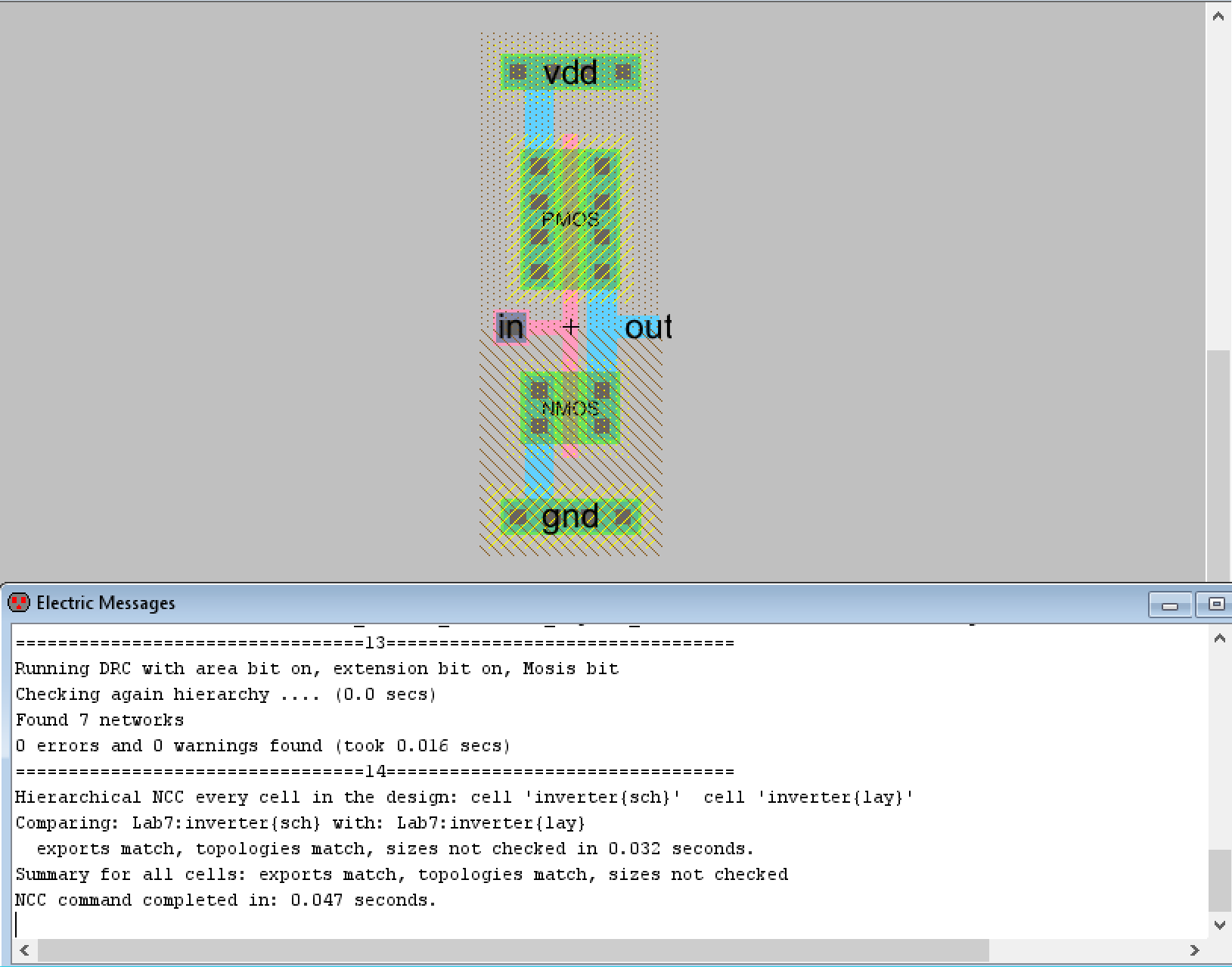
Figure 1. Imported inverter with DRC and NCC check results.
The inverter icon was added to a new schematic for the ring oscillator.
Eleven inverters were lined up in a row using the array function. The
inverters were connected together in a ring structure as seen below in
Figure 2. Spice code was used to verify the ring oscillator was
functioning correctly and the LTSpice waveform can also be seen below.
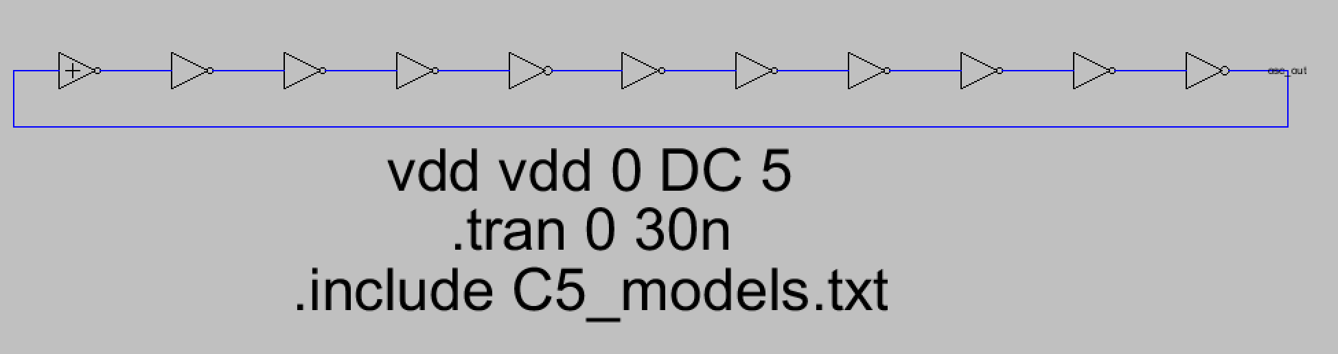
Figure 2. Ring oscillator schematic that is made up of eleven inverters.
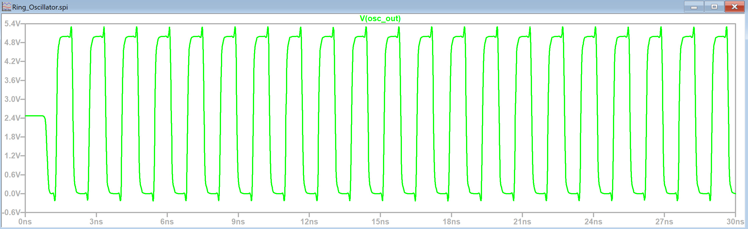
Figure 3. LTSpice simulation waveform of the ring oscillator.
After this another ring oscillator was built by adding a single
inverter to a new schematic called 'Ring_Oscillator_Bus'. This inverter
was renamed to 'inverter[0:10]' which creates eleven inverters in
parallel virtually with only one icon required. Next the input pin and
output pin were connected to the inverter using bus arcs and the
exported pins were called 'osc_out, out[0:9]' and 'out[0:9], osc_out'.
They were named this way because the first inverter takes osc_out as
input, and outputs out[0], then the next inverter will take out[0] as
input and output out[1] and so on. The last inverter takes out[9] as
input and then outputs osc_out which is the input for the first
inverter which completes the ring structure of the oscillator seen in
Figure 2. The completed Ring Oscillator Bus schematic can be seen in
the figure below with DRC check results.
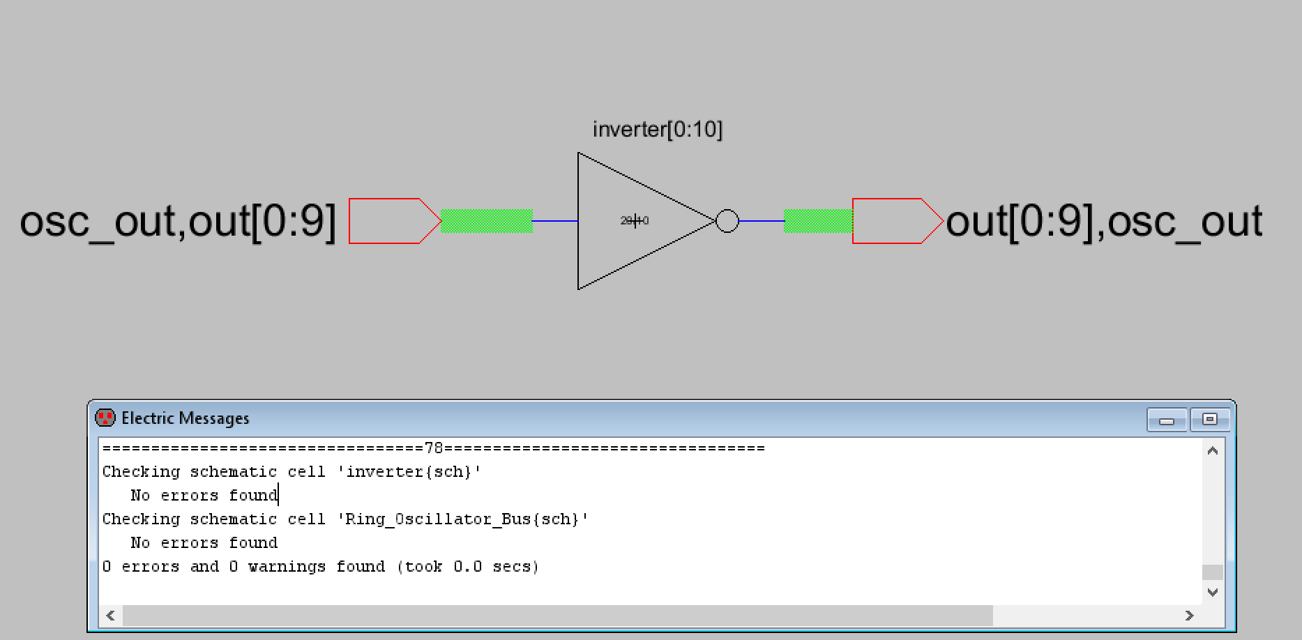
Figure 4. Ring Oscillator Bus schematic with DRC check results.
A simulation was then
performed to verify the functionality is the same as the first ring
oscillator created. The LTSpice simulation waveform looked similar to
the first ring oscillator and can be seen below in Figure 5.
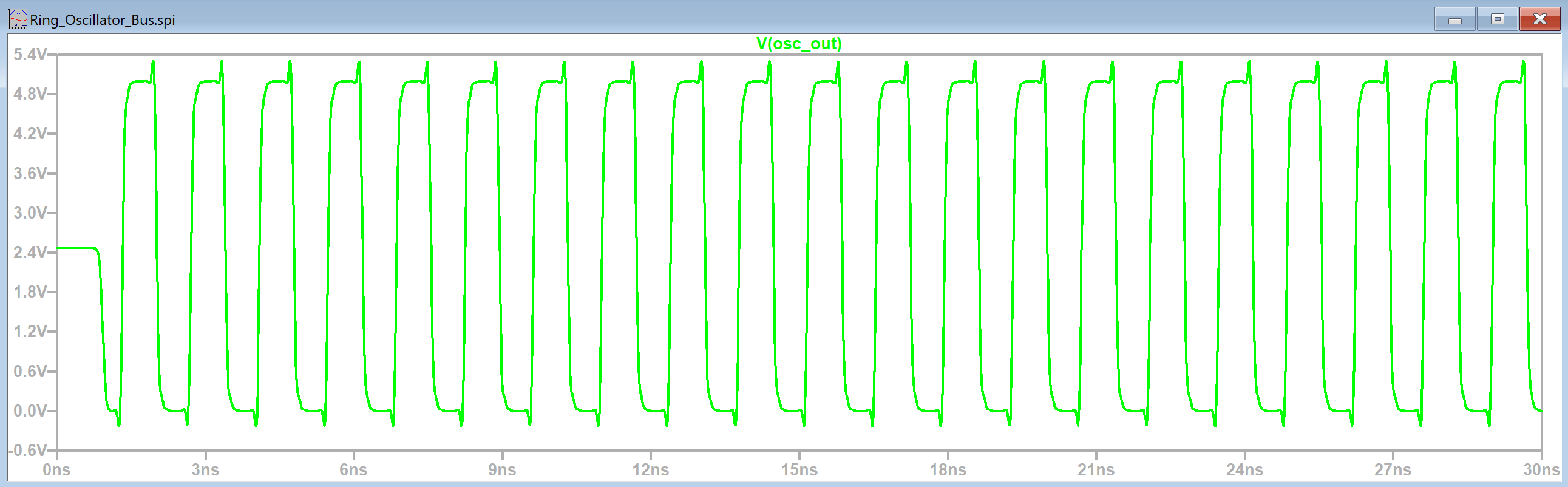
Figure 5. LTSpice simulation waveform of the ring oscillator bus schematic.
Now that the functionality was correct the layout view for the ring
oscillator bus was created. We couldn't use buses like we used them in
schematic view due to the layout view showing how the schematic is laid
out on a physical PCB. We have to manually add the wiring for the
signals instead of relying on Electric VLSI to know there are eleven
parallel inverters. The layout view is similar to the first ring
oscillator schematic in Figure 2 because we will be wiring up the
previous inverter with the next inverter until all eleven inverters are
in series.
The first part of the layout view required us to make the basic
connections between the inverters after adding eleven of them using the
array function. A DRC check was also performed prior to continuing work
on the ring oscillator bus layout view.
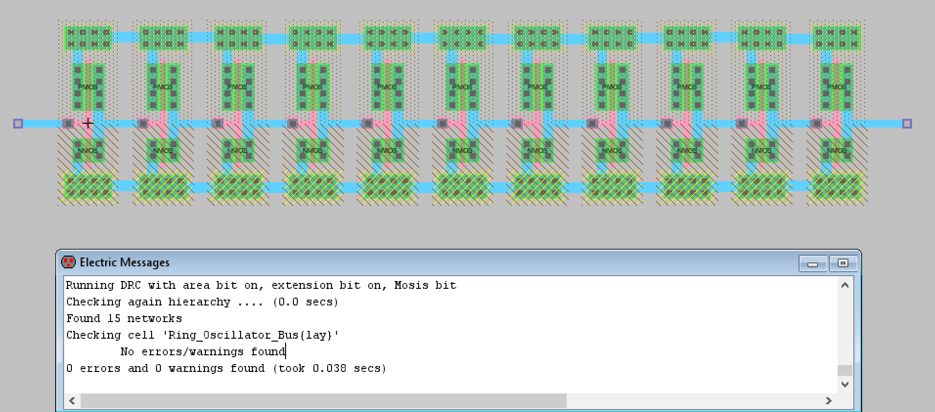
Figure 6. Ring oscillator bus
layout view with the basic connections made between inverters and the
results of a DRC check displayed.
Now that the layout was DRC clean the connections between each inverter
were appropriately exported as out[0] to out[9] with the osc_out export
being the metal2 connection from the first inverter to the last
inverter. VDD and GND were also exported and the layout view
successfully passed the NCC check.
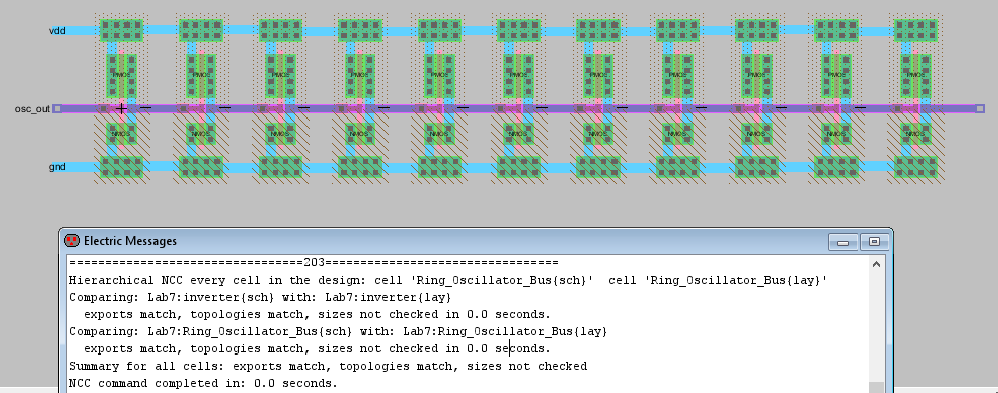
Figure 7. The completed ring oscillator bus schematic with NCC check results.
Task 2: Design an 8-bit AND gate.
For task two I first created the AND gate schematic and icon that
matched the lab's shown AND gate. The schematic, icon, and DRC check
results can be seen in the Figure below.
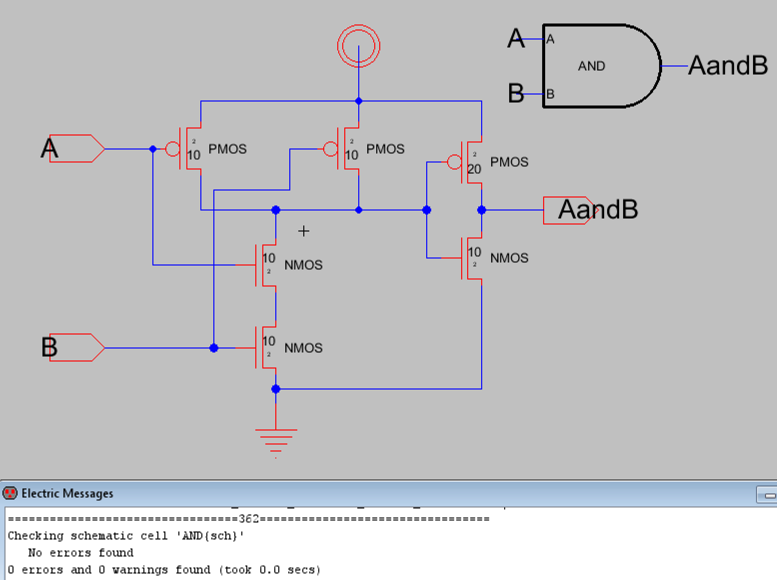
Figure 8. Schematic, icon, and DRC check results for the AND gate.
Now that the AND gate was created the next step was to create a
schematic for an 8-bit AND gate using the icon of the newly created AND
gate along with bus inputs used in the same way the ring oscillator bus
schematic used buses in task one. The icon was added, renamed to
AND[0:7] (for 8 bits total), and input and output pins were exported as
8-bit buses. The A port was exported as A[0:7], the B port was B[0:7],
and the output was exported as AandB[0:7]. They were connected to the
AND gate uses bus arcs too and an icon view was created for the
schematic. The results can be seen in Figure 9 below. A DRC check was
also performed and the results can be seen below.
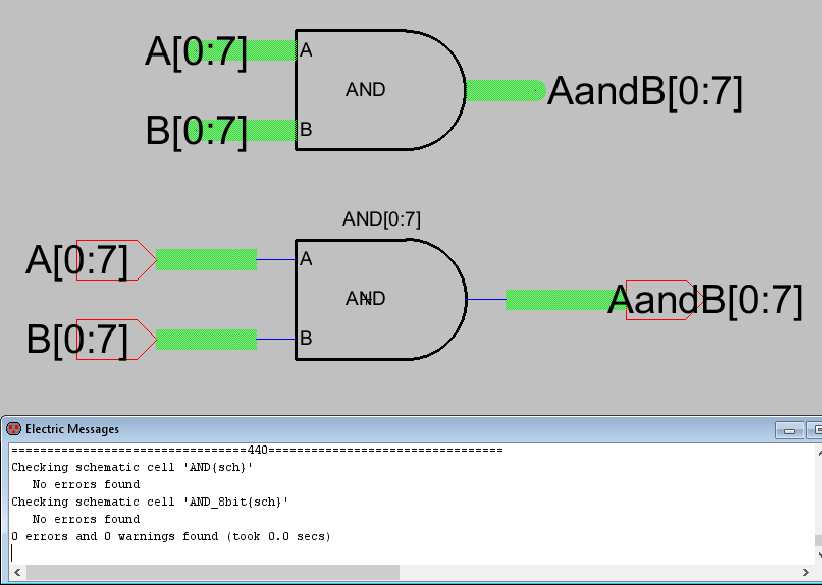
Figure 9. Schematic view and icon of the 8-bit AND gate. The icon is shown above the schematic and DRC check results.
Before moving on to the layout view a schematic for simulating the
8-bit AND gate was created to verify that the design was functioning
correctly. The first simulation set the 8-bit A to all high and the
second set A to all low. B was kept the same for both simulations and
was set to "01010101" starting from B[0]. The first simulation shows
that for the AandB output, only the 2nd, 4th, 6th, and 8th outputs were
high which is correct. The second simulation shows that since A is set
to all low, the AandB output should be all low as well, which shows the
8-bit AND gate is functioning properly. Both LTSpice simulation plots
can be seen below.
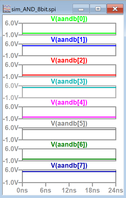
Figure 10. Two simulations of
the 8-bit AND gate. The left plots show AandB output when it is
possible for some outputs to be high while the right shows AandB output
when all outputs should be low.
Now that the functionality of the 8-bit AND gate was verified the
layout view for an individual AND gate had to be created. After
building many layouts in Lab 6 I was able to build the AND gate based
off the schematic with some assistance from the layout shown in the lab
instructions. I created the layout view for the AND gate and verified
it passed DRC and NCC checks as shown below in Figure 11.
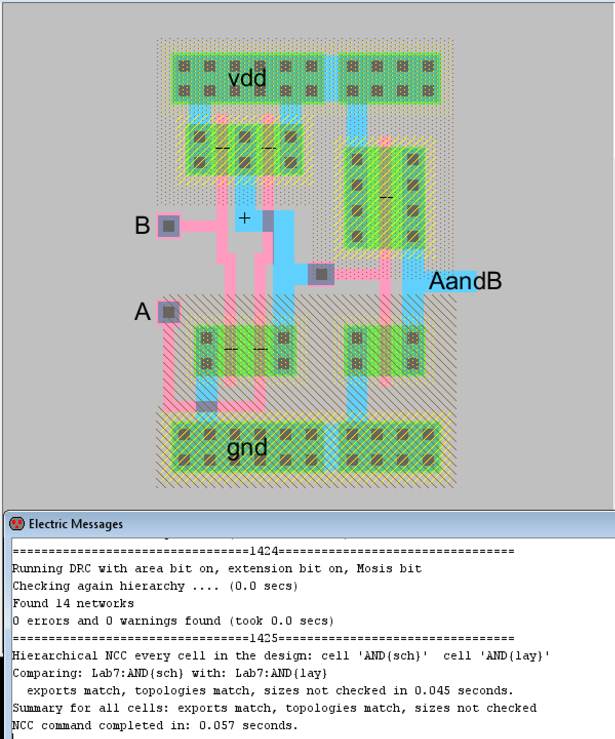
Figure 11. Layout view of the AND gate.
Now that the layout of one AND gate was created, we were then tasked
with creating the layout view for the 8-bit AND gate. The process was
similar to the ring oscillator bus layout. 8 AND gate layouts were put
into the layout view of the 8-bit AND gate and their VDD and GND inputs
were connected together. Since the 8-bit AND gate does bitwise AND
operations the inputs and output for each AND gate had to be exported
as A[n], B[n], and AandB[n] where n is 0 to 7. The completed AND gate
with DRC and NCC check results can be seen below in Figure 12. A closer
view of how the AND gates were connected together can be seen in Figure
13.
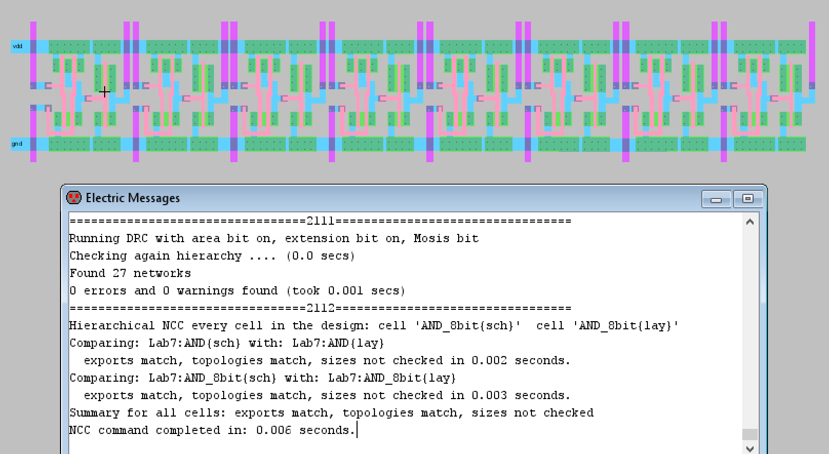
Figure 12. Completed layout view of the 8-bit AND gate with good DRC and NCC check results.
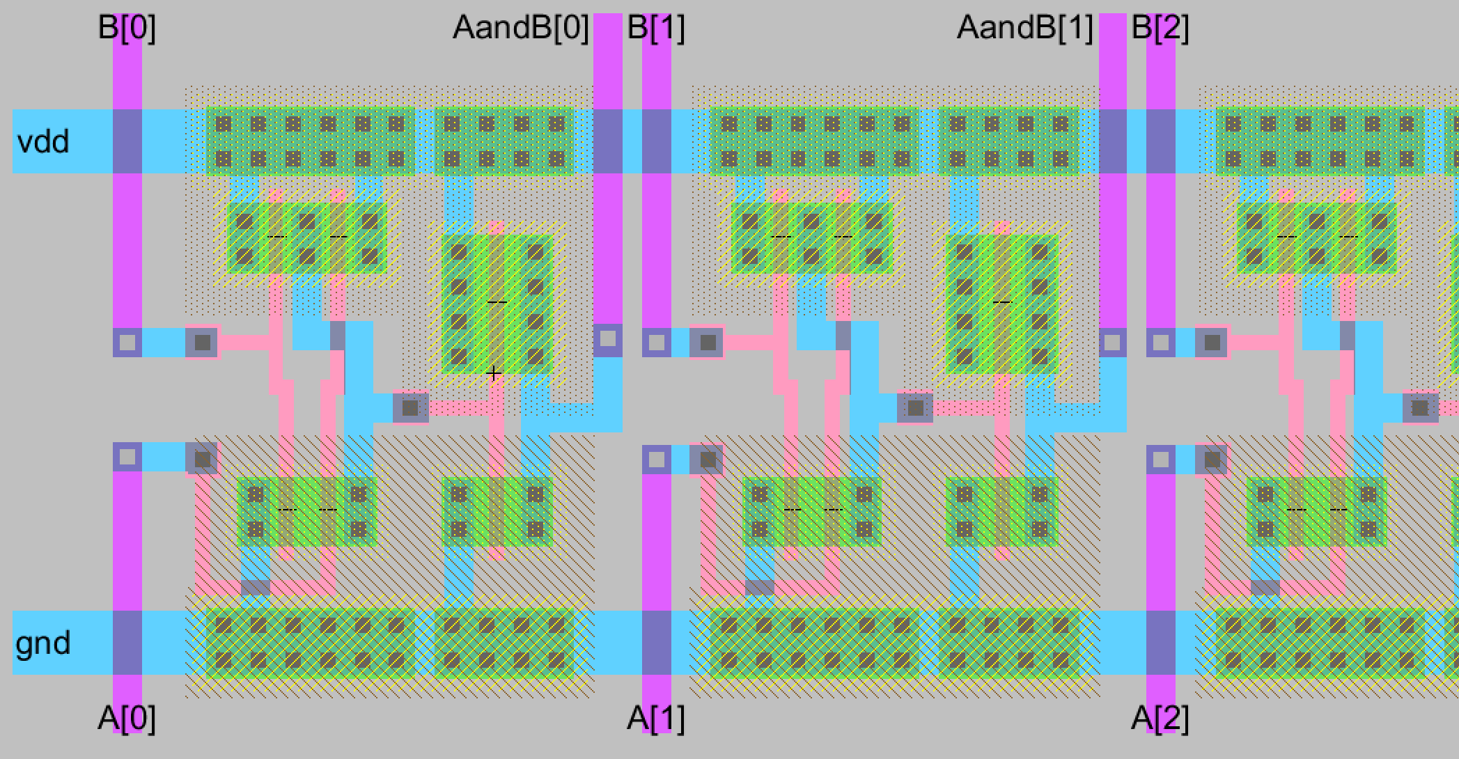
Figure 13. A closer view of how the AND gates are connected together and of the exported input pins and output pins.
Task 3: Design an 8-bit OR gate.
The first step for designing the 8-bit OR gate was to create the
schematic and icon of an individual OR gate. The schematic, icon, and
DRC check results for my OR gate can be seen below in Figure 14.
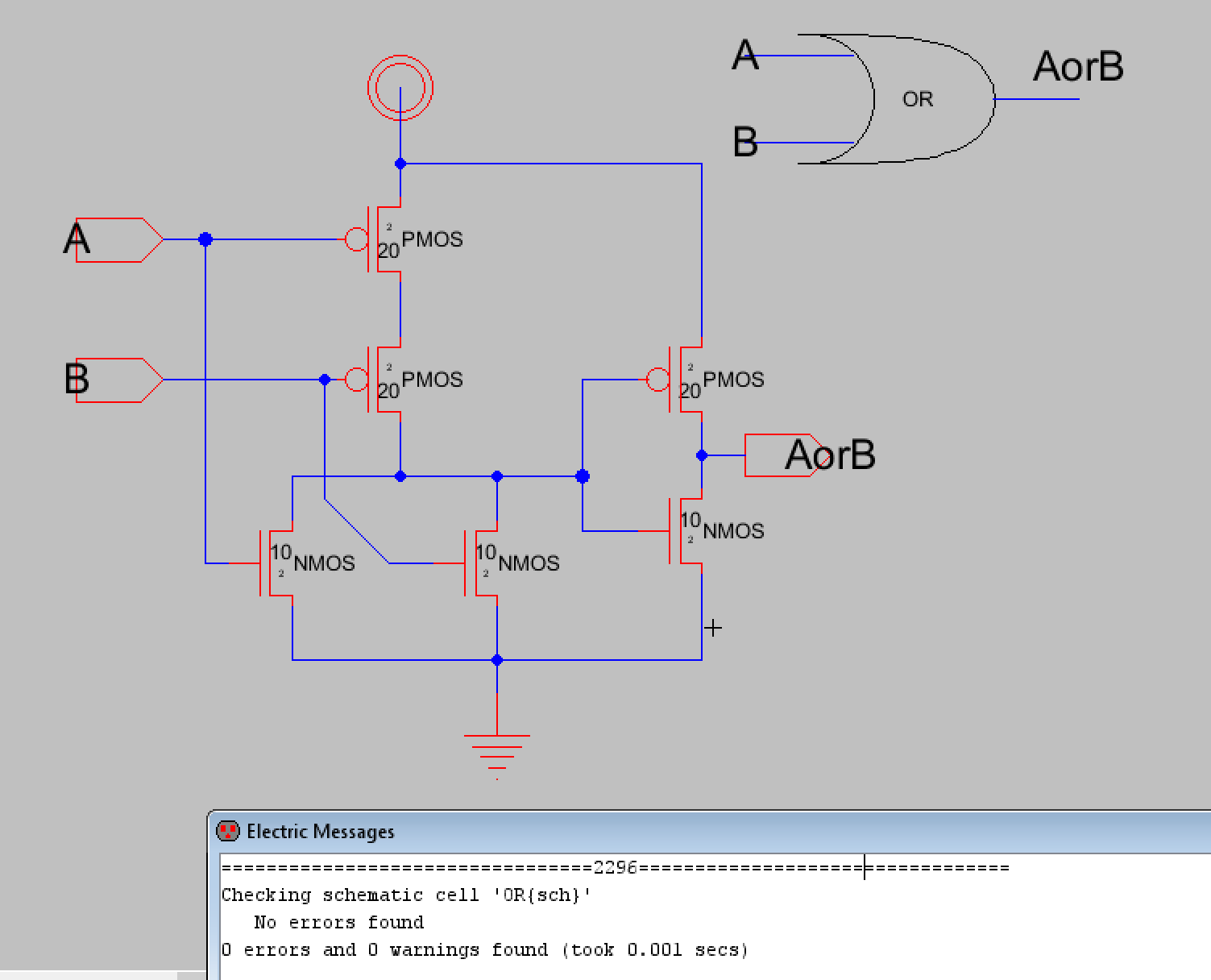
Figure 14. Schematic, icon, and DRC check results for my OR gate.
A simulation of the individual OR gate was also performed to verify it
was functioning correctly. The simulation schematic and LTSpice
simulation waveform can be seen below in Figures 15 and 16.
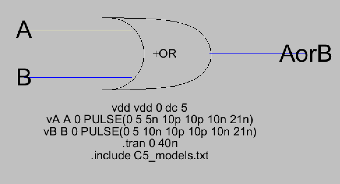
Figure 15. Simulation schematic for the individual OR gate.
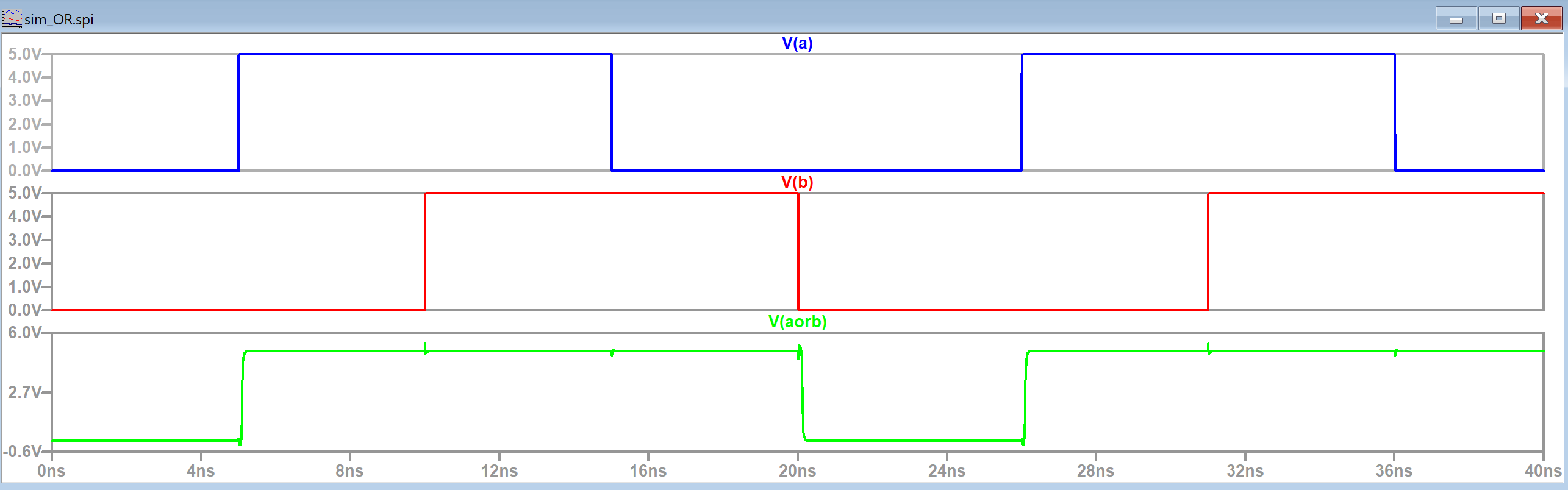
Figure 16. LTSpice simulation waveform for the individual OR gate.
After verifying the OR gate's functionality the layout view of the
individual OR gate was created. DRC and NCC checks were performed
before moving on to creating the 8-bit OR gate.
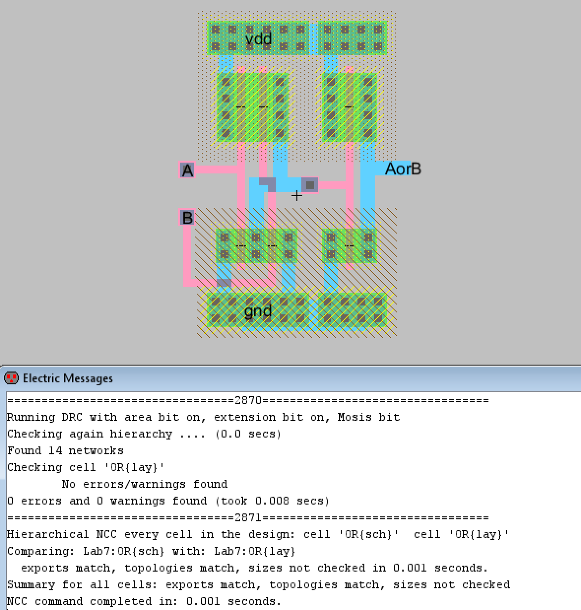
Figure 17. The layout view for an individual OR gate.
Now the schematic and icon for the 8-bit OR gate was created. It uses
buses like the previous 8-bit AND gate and ring oscillator. Inputs were
exported as A[0:7] and B[0:7] just like the AND gate and the output was
exported as AorB[0:7]. The schematic and icon are shown below.
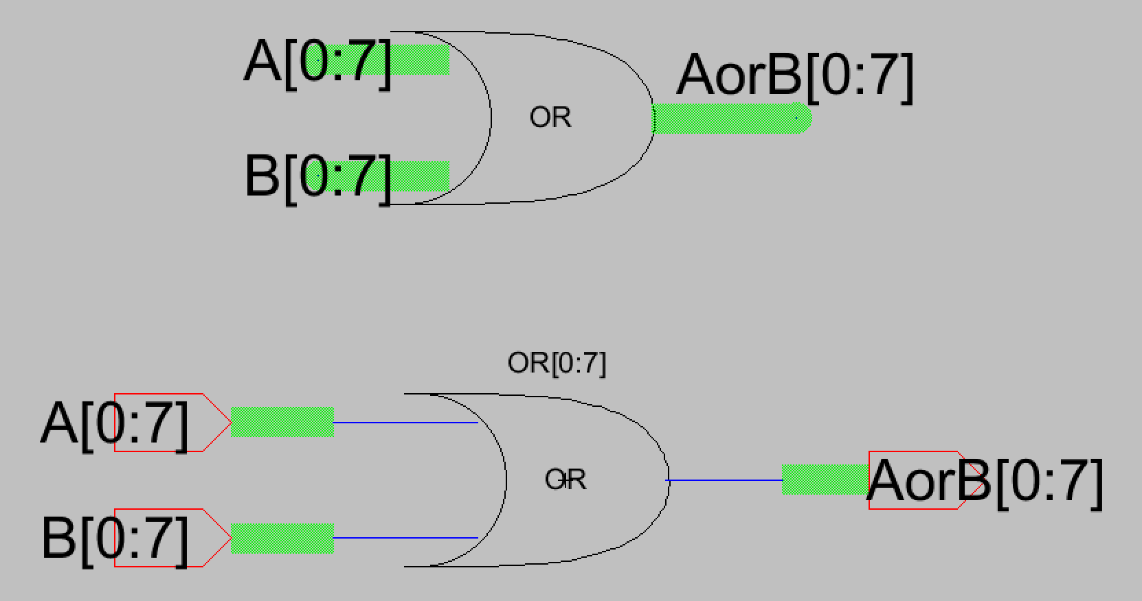
Figure 18. Icon and schematic for the 8-bit OR gate.
A simulation to verify the logic of the OR gate was also performed.
Figure 19 displays the simulation schematic that was used. A was set to
low while B kept the same "01010101" pattern as before. It was expected
that the output should match the B input since A is set to low and this
is what is seen in the LTSpice simulation shown below.
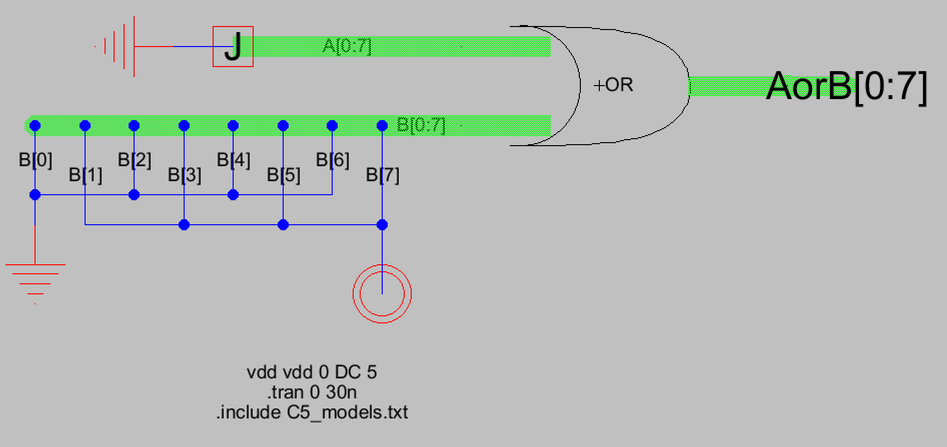
Figure 19. Simulation schematic for the 8-bit OR gate.
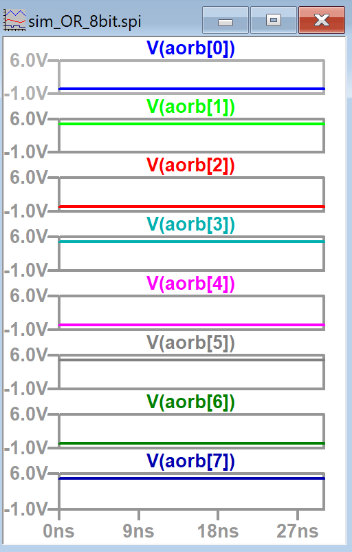
Figure 20. LTSpice plots of the AorB outputs. The outputs match the B input as expected.
Now the layout view for the 8-bit OR gate could be created. The results
are shown below in Figure 21. The process was similar to the 8-bit AND
gate and DRC and NCC check results can also be seen. Figure 22 shows a
closer look at the 8-bit OR gate layout structure.
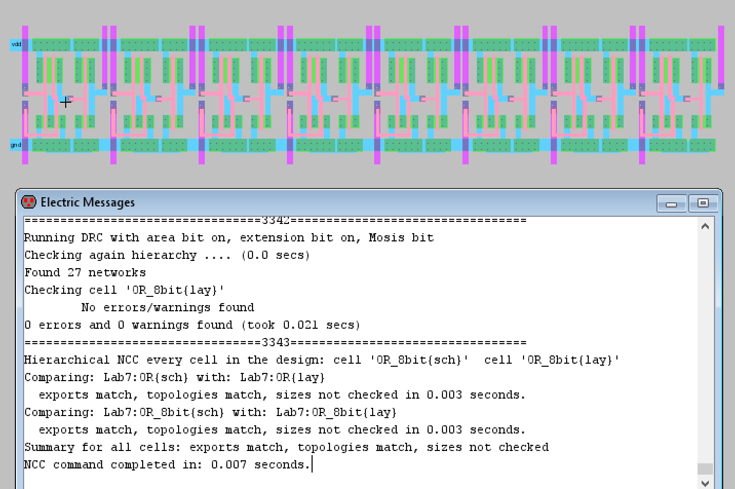
Figure 21. Final layout view for the 8-bit OR gate.
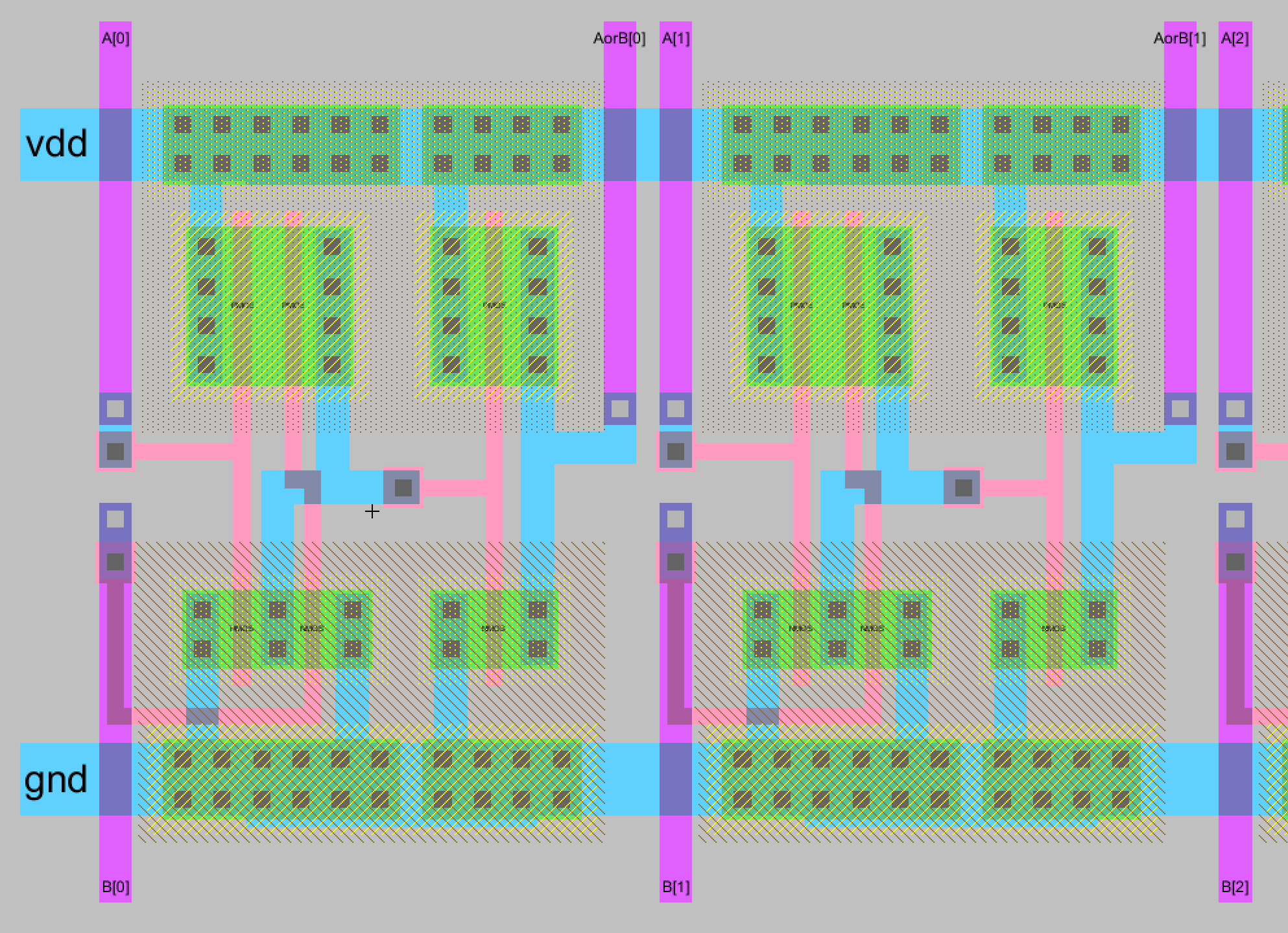
Figure 22. A closer look at the 8-bit OR gate and how the pins were laid out and exported.
Task 4: Design an 8-bit NAND gate.
The schematic and icon of a NAND gate was successfully created. It can
be seen below in Figure 23 along with DRC check results. I opted to
create another NAND gate to get more practice with the layout view
instead of importing the NAND gate created in a previous lab.
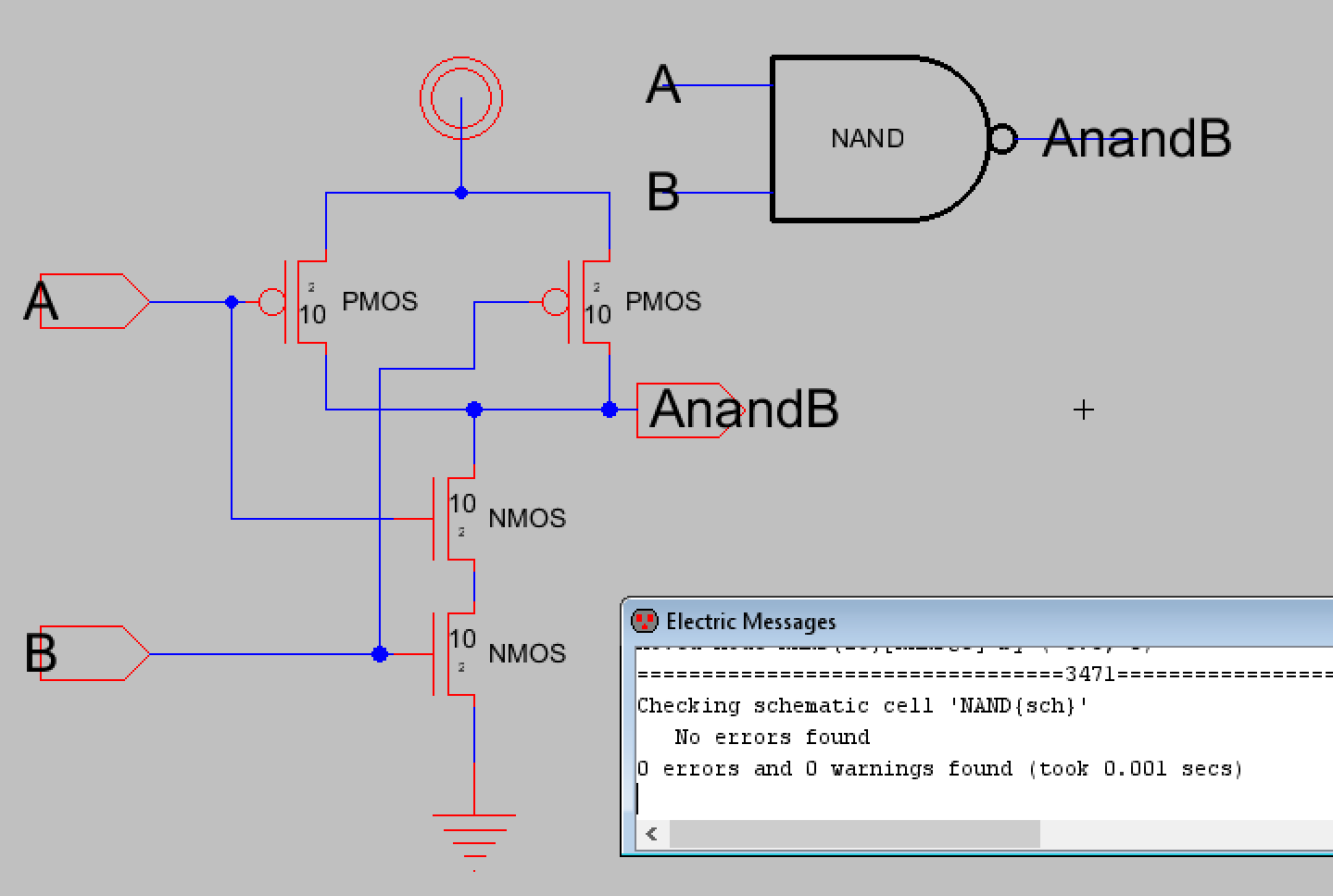
Figure 23. Schematic, icon, and DRC check results for the NAND gate.
After this I created the layout view for the individual NAND gate and made sure it passed DRC and NCC checks.
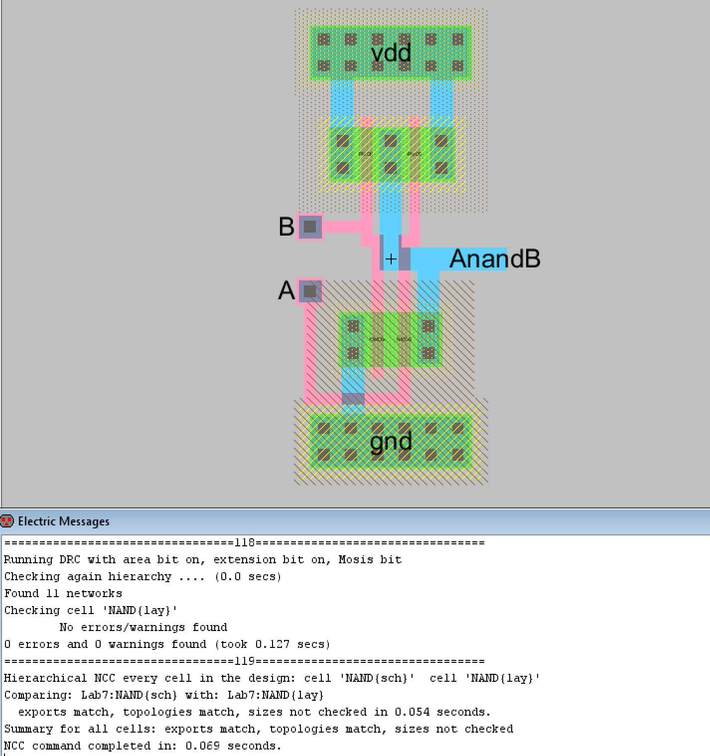
Figure 24. Layout view of the individual NAND gate with DRC and NCC check results.
Next the schematic and icon of the 8-bit NAND gate was created and a
simulation was ran to verify the logic was correct. The schematic and
icon can be seen in Figure 25. Figure 26 shows the simulation schematic
used and Figure 27 displays the LTSpice simulation plots for AnandB
outputs.
The 8-bit NAND schematic and icon were verified to be DRC clean before
proceeding. The simulation schematic uses the same setup as the
previous simulations and according to the LTSpice simulation plots, the
8-bit NAND gate is functioning correctly.
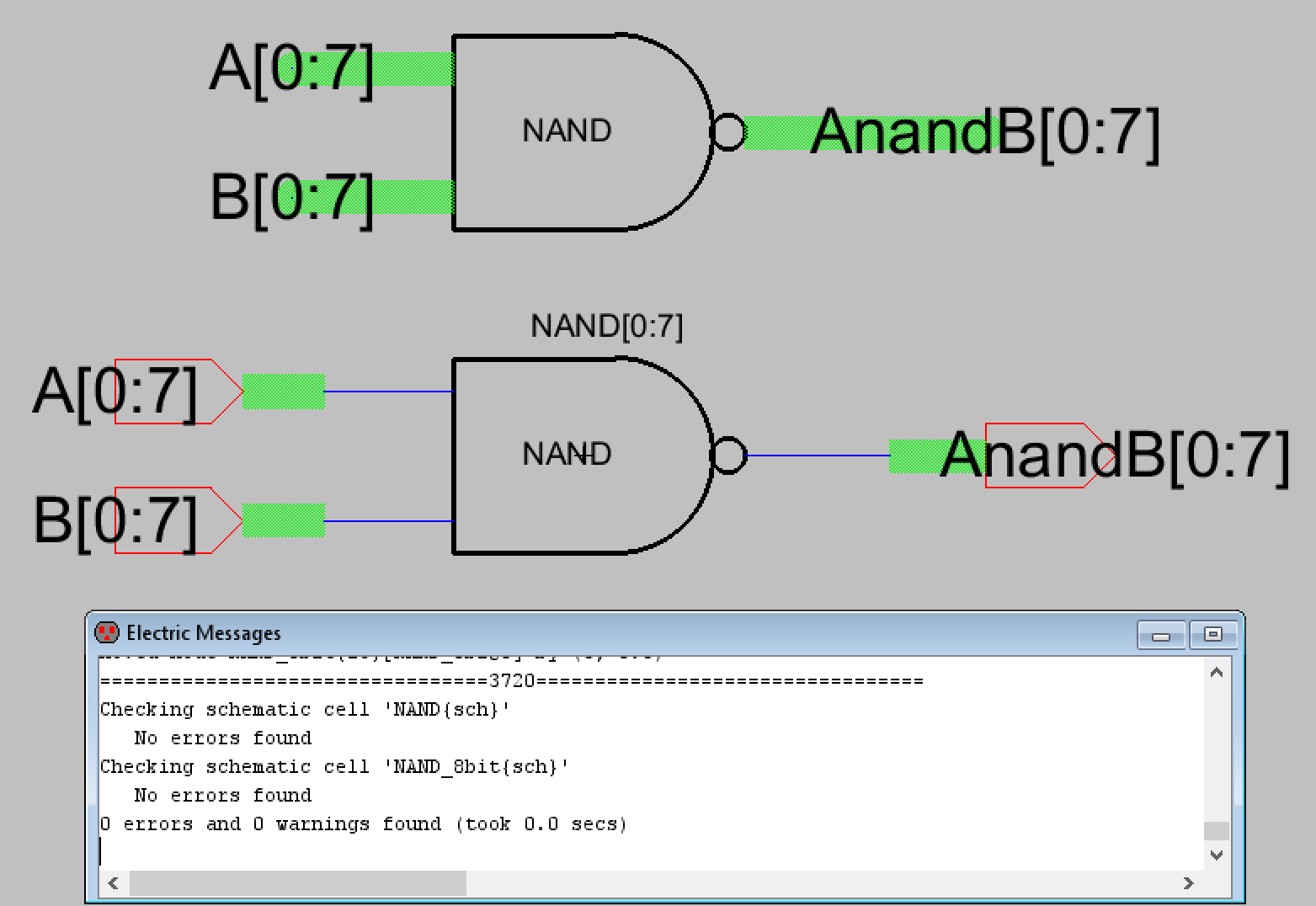
Figure 25. Icon and schematic for the 8-bit NAND gate with DRC check results.
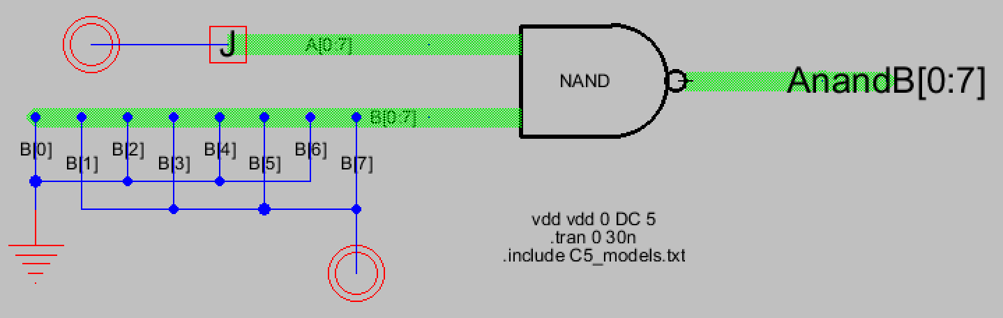
Figure 26. Simulation schematic for the 8-bti NAND gate.
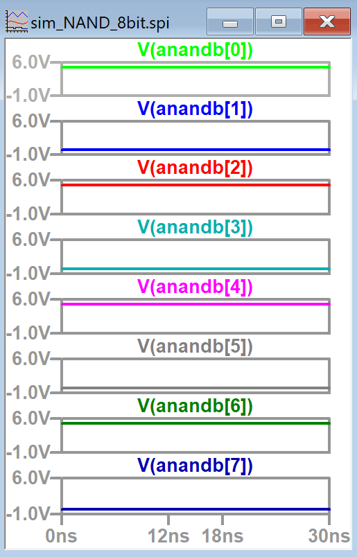
Figure 27. LTSpice simulation plots for the 8-bit NAND gate outputs.
Now the layout view for the 8-bit NAND gate was completed and can be
seen below in Figure 28 in addition to DRC and NCC check results. The
process was the same as previous 8-bit gates. Figure 29 shows a closer
look at how the input and output pins were laid out.
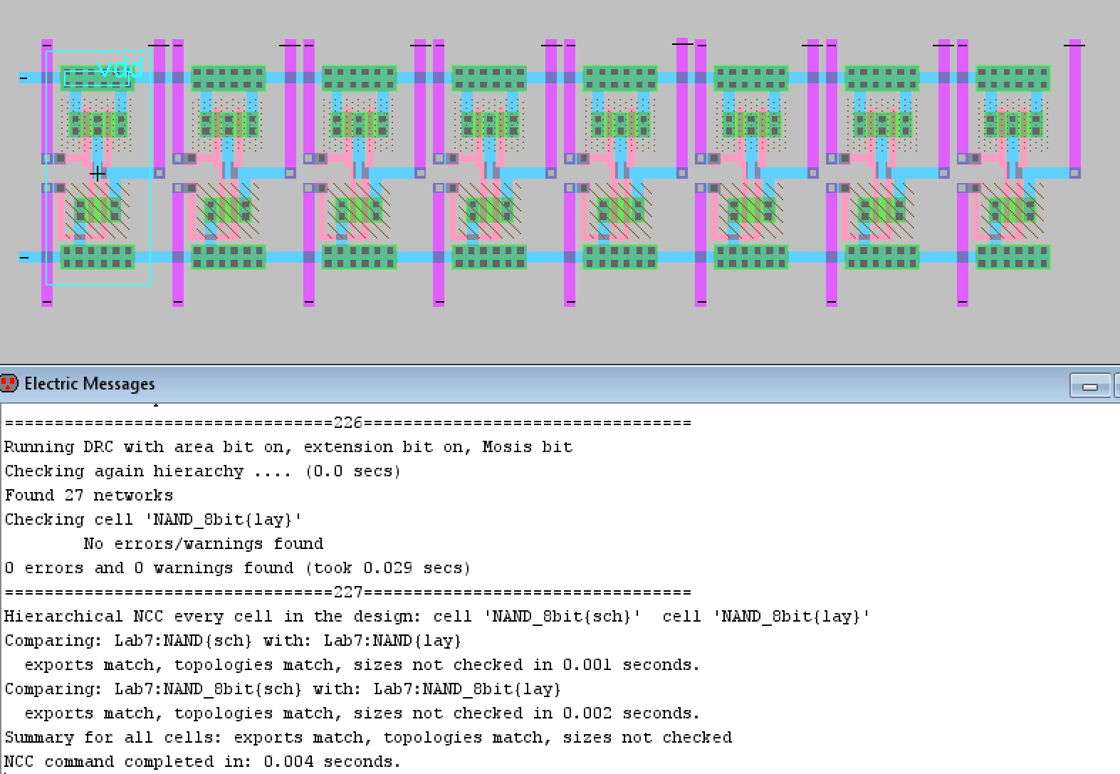
Figure 28. Final 8-bit NAND gate layout view with good DRC and NCC check results.
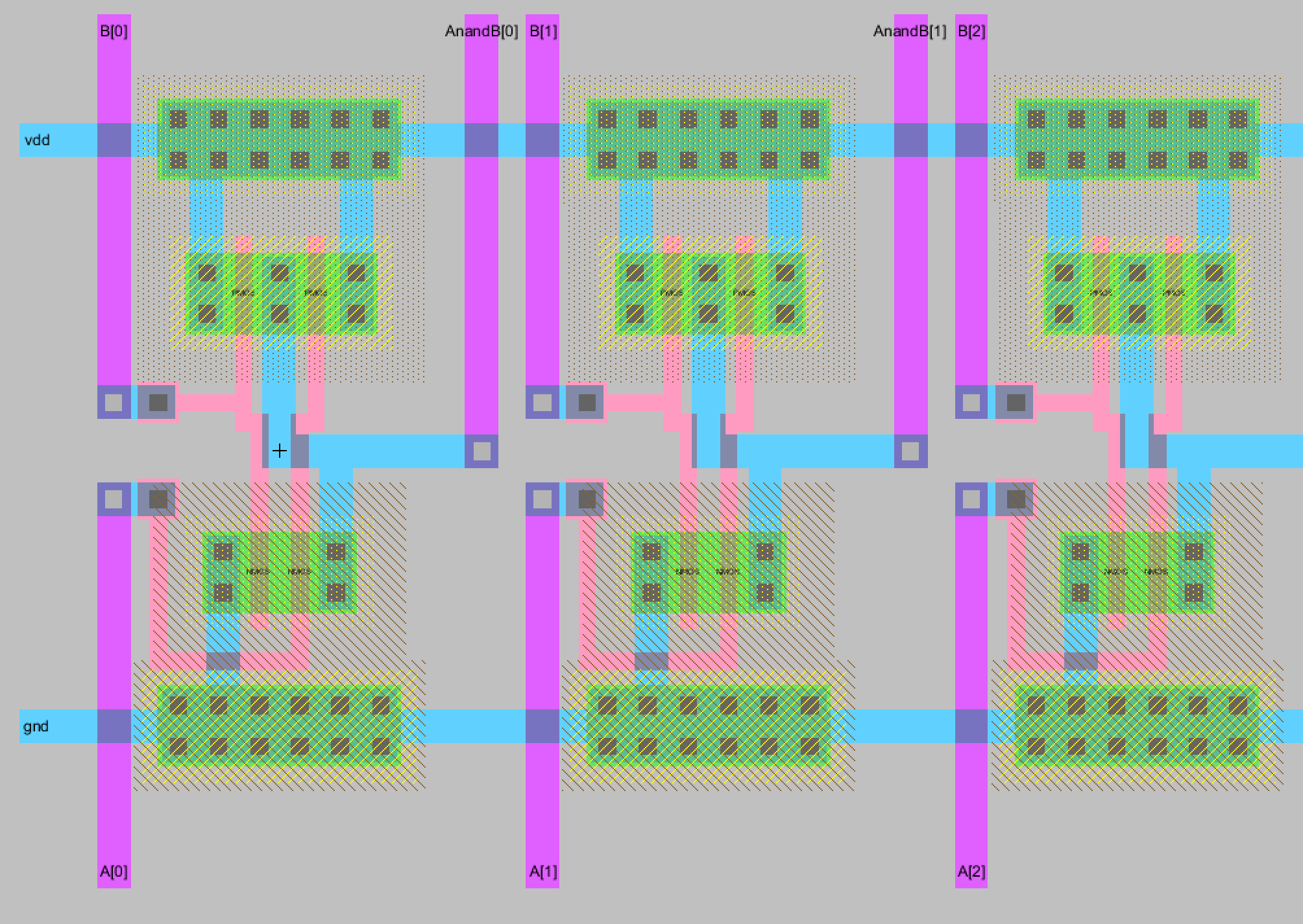
Figure 29. Closer look at the 8-bit NAND gate layout.
Task 5: Design an 8-bit NOR gate.
The final 8-bit logical gate to be designed was the NOR gate. The
individual NOR gate's schematic and icon with DRC check results is
shown below in Figure 30. The layout view for the individual NOR gate
is also shown below in Figure 31 with its DRC and NCC check results.
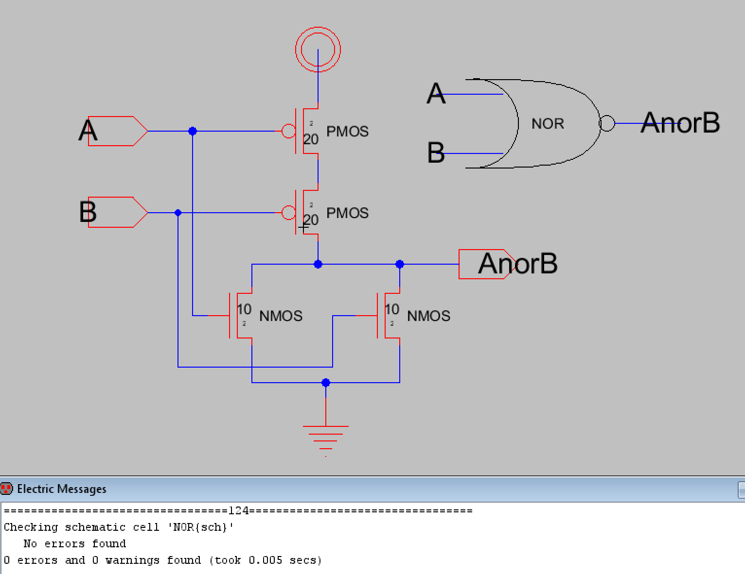
Figure 30. Schematic, icon, and DRC check results for the NOR gate.
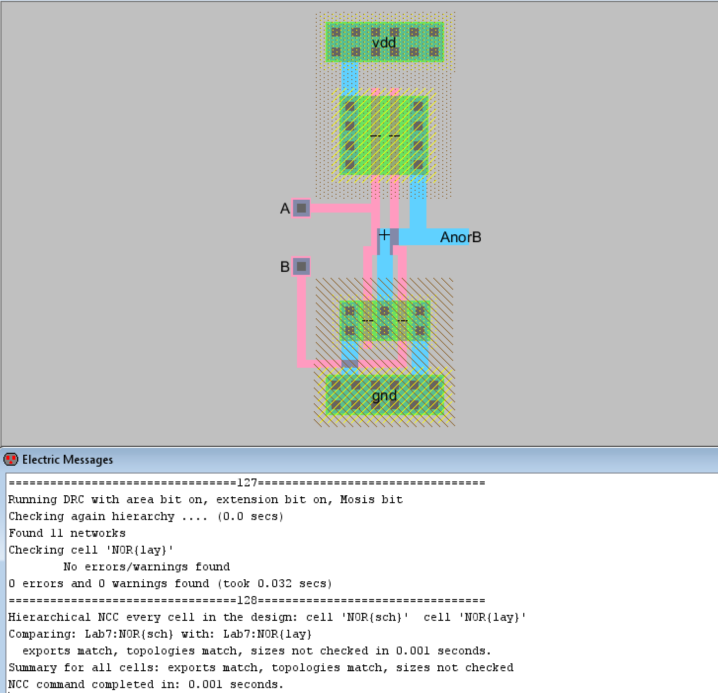
Figure 31. Layout view of the individual NOR gate with good DRC and NCC check results shown.
The 8-bit NOR gate schematic and icon was created in the same process
as before. The schematic and icon can be seen below in Figure 32. It
was also verified to be DRC clean before proceeding.
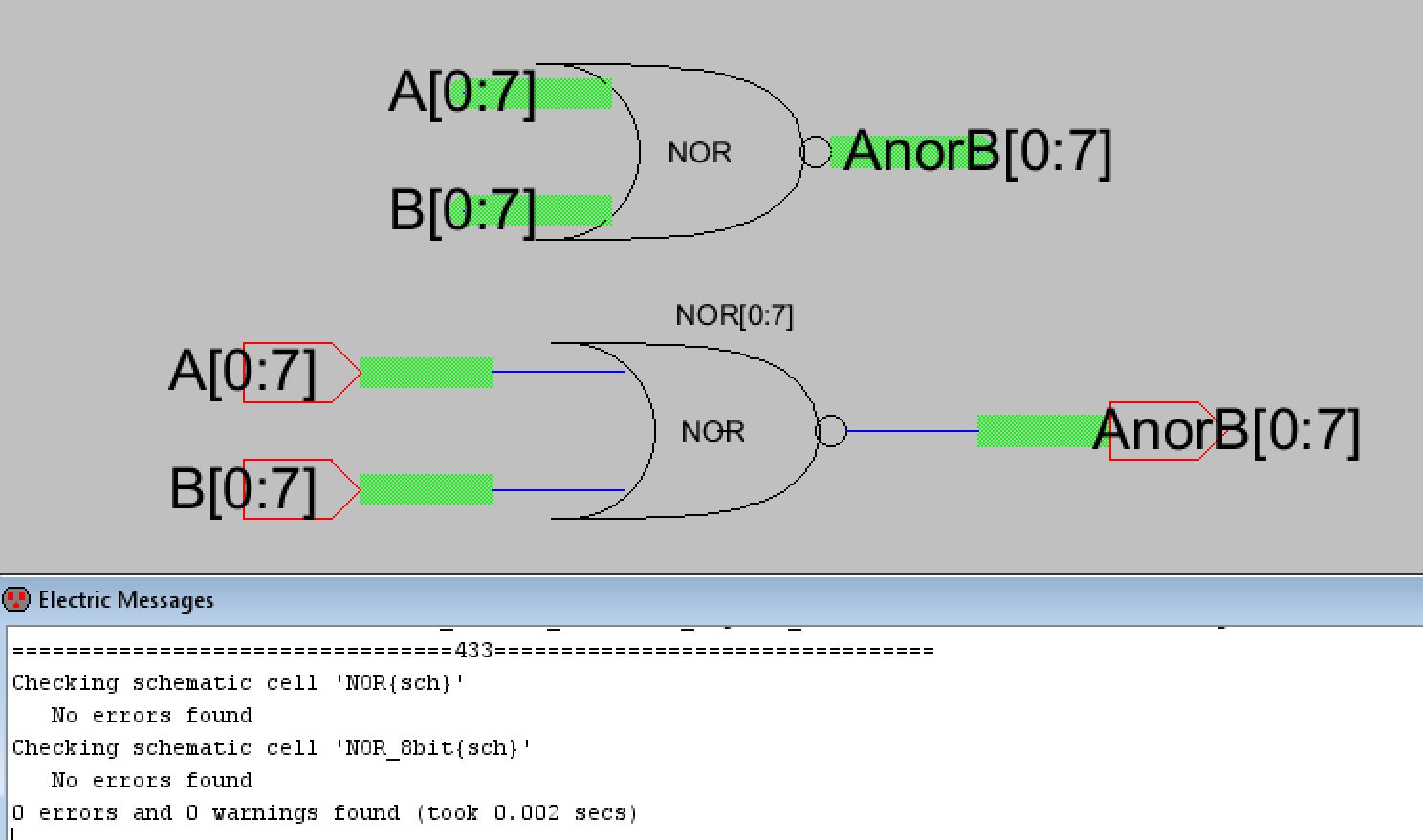
Figure 32. Schematic, icon, and DRC check results for the 8-bit NOR gate.
A simulation schematic was created to verify the NOR gate's logic. The
simulation schematic and LTSpice plots can be seen below in Figures 33
and 34. The setup is identical to the previous simulation setups except
A is set to be all low in this case because a NOR gate output is only
high if both inputs are zero. The LTSpice simulation verified the 8-bit
NOR gate was functioning correctly.
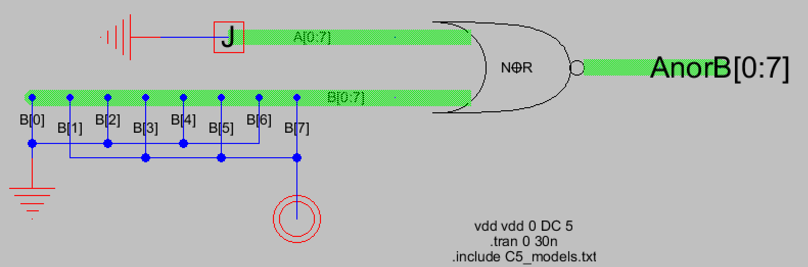
Figure 33. Simulation schematic for the 8-bit NOR gate.
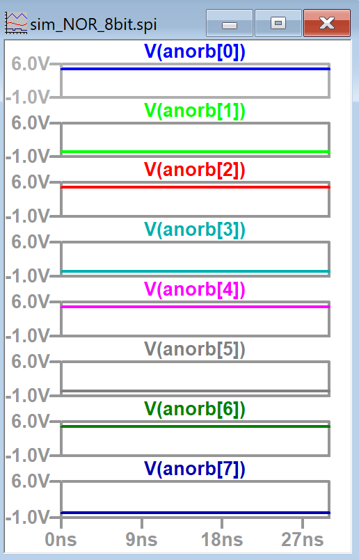
Figure 34. LTSpice simulation plots for the AnorB outputs. Results are what was expected.
Now that logic was verified the layout view for the 8-bit NOR gate was
completed. Figure 35 shows the completed layout view with DRC and NCC
check results. Figure 36 also shows a closer look at the 8-bit NOR
gate's layout view.
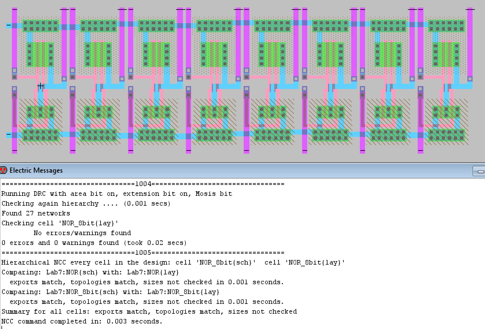
Figure 35. Final layout view for the 8-bit NOR gate with good DRC and NCC check results displayed.
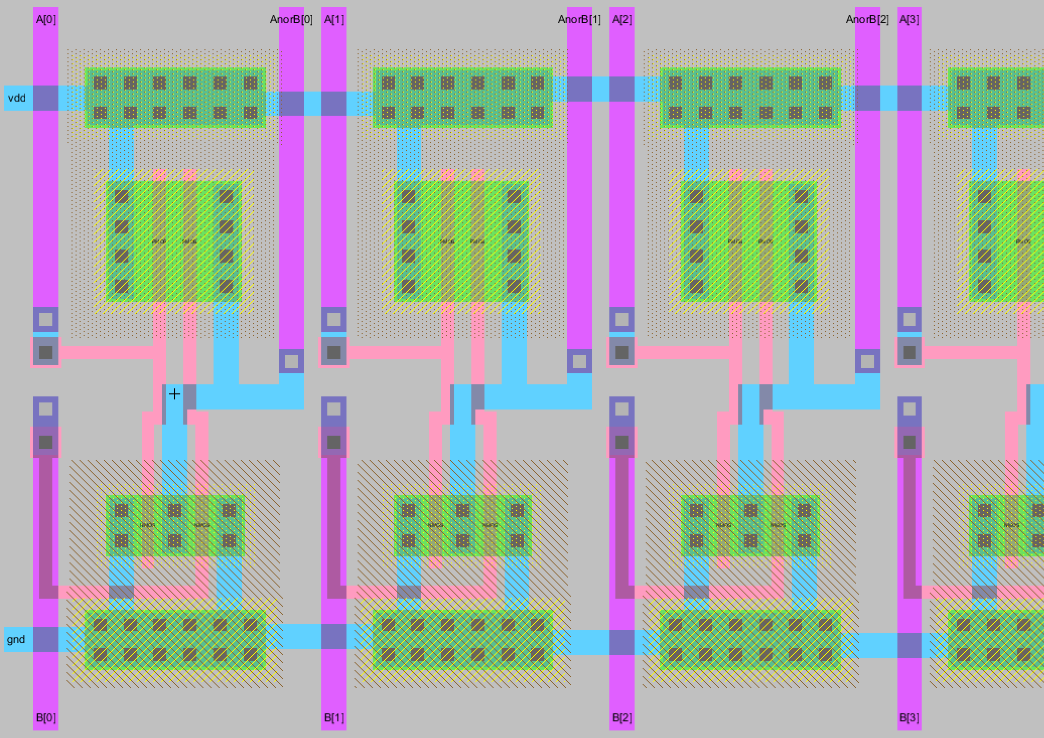
Figure 36. Closer look at the layout view for the 8-bit NOR gate.
Discussion
This lab was enjoyable for me because it made me much more comfortable
using the layout view and learning how to troubleshoot issues when the
NCC check doesn't pass. There was one persistent issue I kept running
into when I tried to simulate the 8-bit logical gates. I wasn't aware
that individual wires should be renamed to things like B[0] and the
buses had to be renamed to A[0:7] and B[0:7]. I wasn't able to simulate
the designs in LTSpice until I was informed of that requirement by my
professor. I knew the designs worked however since I used the built in
simulator, ALS, to verify and I also knew the individual logic gates
functioned correctly. I also learned to pay much more attention to the
schematic when designing the layout, there were multiple times where
NCC didn't pass only because I mixed up my input pins and so the layout
didn't match the schematic. I also noticed that the NAND and NOR gate
layouts went by very quickly compared to the start of the lab since I
had become so familiar with the process of turning individual gates
into 8-bit gates. This lab was also pretty time consuming since most of
the gates had to be created from scratch and even the ones that didn't
have to, I opted to so that I could gain more practice using Electric
VLSI.