ENGR338 Lab 2021
Spring
Lab 5 The Inverter
Name: Sean
Eaton
Email:
smeaton@fortlewis.edu
Introduction
In this lab we were tasked with building an inverter in Electric VLSI.
The inverter schematic should be first created and then the layout
view. After the first inverter had been created we then had to build a
larger inverter using the Multiplier function and editing the layout
view to contain 5 PMOS and 5 NMOS transistors. LTSpice simulations were
ran to confirm the inverter was functioning correctly. After this two
new simulation tools were then introduced, one of which had to be
installed.
Task 1: Create the schematic of the inverter.
For task 1 we had to create the schematic view of the inverter using a
PMOS and NMOS transistor. The PMOS transister should have its width set
to 20 and its length set to 2. The NMOS transister should have its
width set to 10 and its length set to 2. The PMOS should also be
orientated with its drain oriented down to the NMOS transistor. The VDD
and GND symbols should be used as well as exported 'in' and 'out' ports
for the inverter and the icon view should be created. After this a DRC
check should be run along with setting the spice models for the PMOS
and NMOS transisters. Finally the schematic should be tested using the
provided spice code and then tested again using a transient analysis
spice code written by us. The final schematic view should look like the
one shown in Figure 1 below.
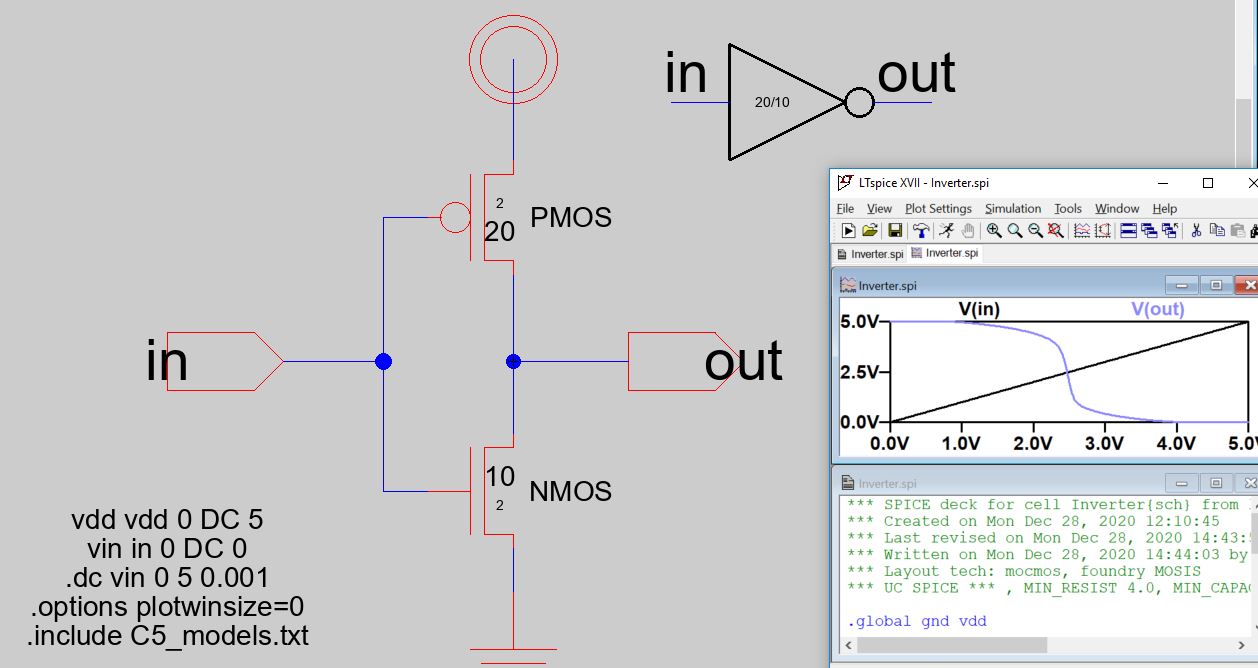
Figure 1. Final schematic
view of the inverter. Its icon view is also shown as well as the first
LTSpice simulation code that was provided.
Task 2: Create the layout of the inverter.
A seperate tutorial was used for this task. The following nodes should
be placed in the layout view: nWell, 2 pActs, pMos, 2 nActs, nMos, and
a pWell node. The spice models need to be set for the pMos and nMos
nodes as well as their lengths and widths to match the schematic view.
Next the nodes should be rotated and moved into position similar to the one shown in Figure 2.
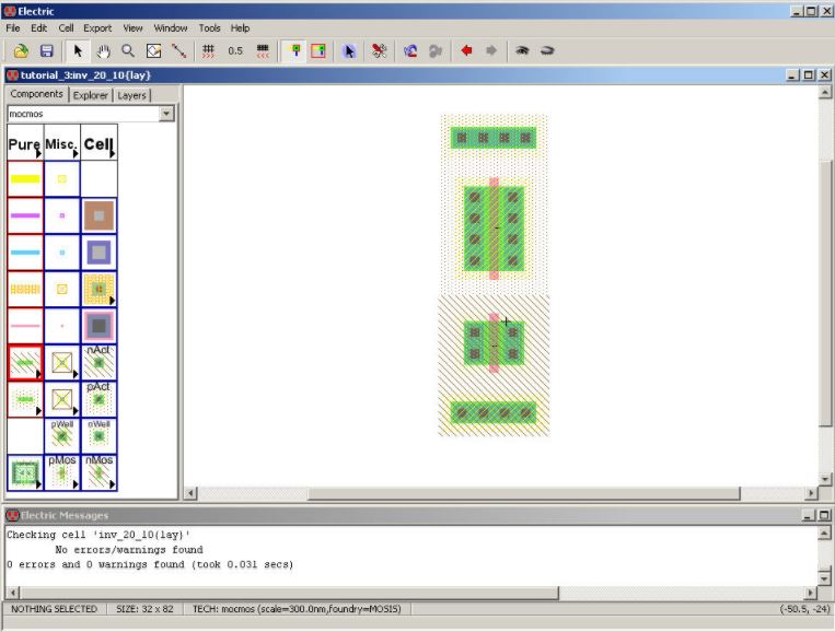
Figure 2. Layout view of the inverter with the edited nodes moved into position.
After this the two poly gates should be connected, the metal on the
right of the devices connected, and the metals on the left of the
transistors as shown below in Figure 3. A metal1 contact and metal1 pin
should also be added to the left and right as seen below. Next the
appropriate pins should be exported. The final layout view should look
like the one seen in Figure 3 below. It should pass DRC and NCC checks
as well.
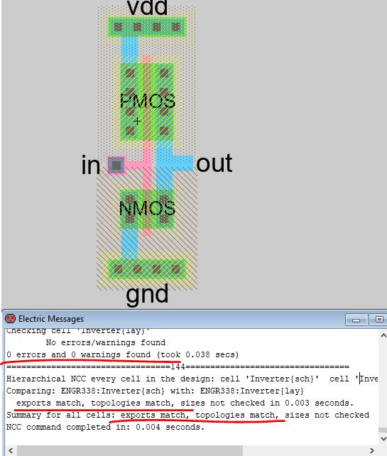
Figure 3. Final layout view for the inverter.
Task 3: Use the multiplier to build a larger inverter.
For task 3 the multiplier function was used to build a 100/2 and 50/2
inverter using copies of the schematic and layout views already created
in tasks 1 and 2.
The new inverter cell should be named 'Inverter_100_50' and the
multiplier for the PMOS and NMOS symbols set to 5. It should look like
the schematic shown in Figure 4 below.
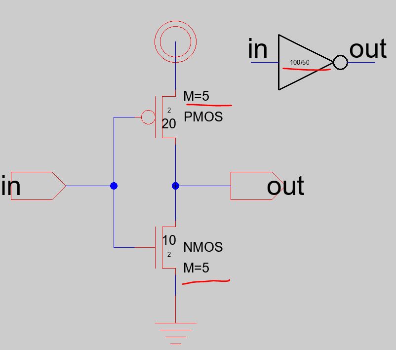 Figure 4. Schematic view of the inverter with the multiplier set to 5.
Next the layout view should be modified as well. The existing
connections should be removed so that the PMOS and NMOS nodes can be
copied and pasted correctly. There should be 5 PMOS and 5 NMOS in
parallel and the VDD and GND should be modified to be wider. The layout
view for the 100/50 Inverter should look like the one shown in Figure 5
below.
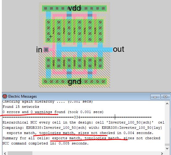
Figure 5. Layout view of the 100/50 inverter.
Task 4: Run simulations to verify the driving capability of these two different inverters.
A new schematic view should be created and named 'sim_inverter' so that
the inverter can be simulated using spice code. The schematic should
look like the one shown in Figure 6 which displays a 100 fF capacitor
connected to ground and to the out pin of the 20/10 inverter.
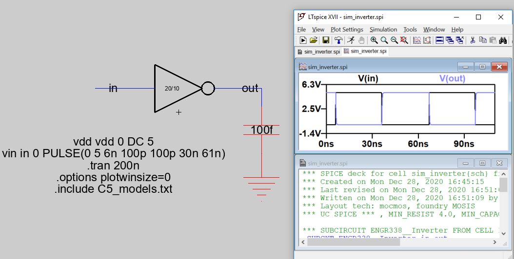
Figure 6. Simulation schematic and LTSpice simulation results for the 20/10 inverter.
The 20/10 inverter and the 100/50 inverter should both be simulated
with a 100 fF, 1 pF, and 10 pF capacitors to compare how the inverter
performance differs between the two inverters.
Task 5: Use a different simulation tool.
In task 5 we had to create a new simulation schematic that contained
both the 20/10 and the 100/50 inverters with two outputs, one for each.
It should look like the schematic shown in Figure 7.
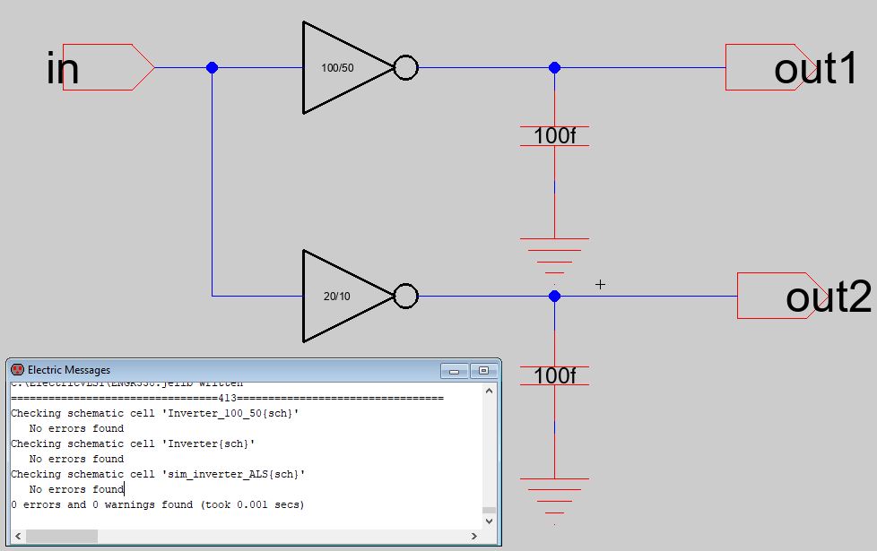
Figure 7. Simulation schematic that contains both the 20/10 inverter and the 100/50 inverter.
After this the cell simulation was performed using a new simulation
tool we hadn't used before. The first one ALS and can be found under
Tool -> Simulation (built-in) -> ALS: Simulate the current cell.
The simulation window should look like the one shown in Figure 8. The
in signal can be directly manipulated by pressing v to set the cursor's
point to high and g to set the point to low.
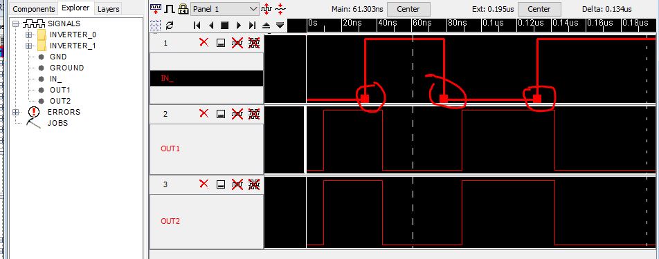
Figure 8. ALS Simulation window.
The next new simulation tool is called IRSIM and its plugin had to
first be installed. The plugin .jar file had to be downloaded and then
the command prompt used to install the plugin. The command prompt
should look like Figure 9. After installation IRSIM could be run like
the ALS simulation and functions in a similar way. IRSIM is shown in
Figure 10.
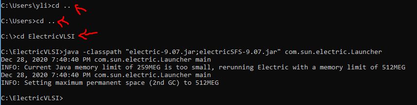
Figure 9. IRSIM installation command in the command prompt.
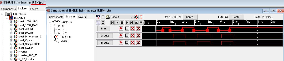
Figure 10. IRSIM Simulation window.
Results
Task 1: The inverter schematic was successfully built using the PMOS
and NMOS transistors, the VDD symbol, the ground symbol, and the in and
out ports. The icon view was also successfully created. Figure 11 shows
the schematic view along with the icon view and DRC check results.
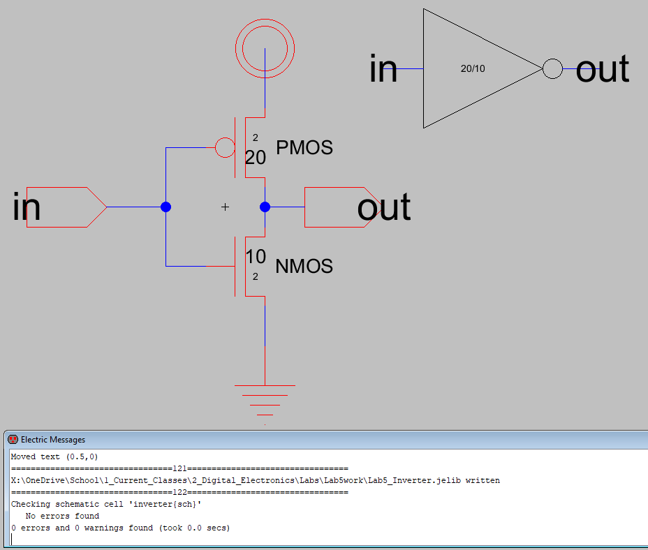
Figure 11. The inverter schematic with its icon and DRC check results.
The first LTSpice simulation that had its spice code provided was also
successfully ran. The LTSpice plot results are shown in Figure 12.
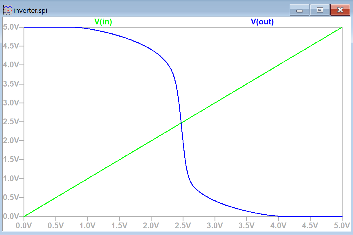
Figure 12. LTSpice simulation plot of V(in) and V(out). The inverter successfully inverts voltage.
LTSpice code for the transient analysis was also successfully written
and an additional DRC check was performed. The spice code as well as
the simulation plot is shown below in Figure 13 and Figure 14.
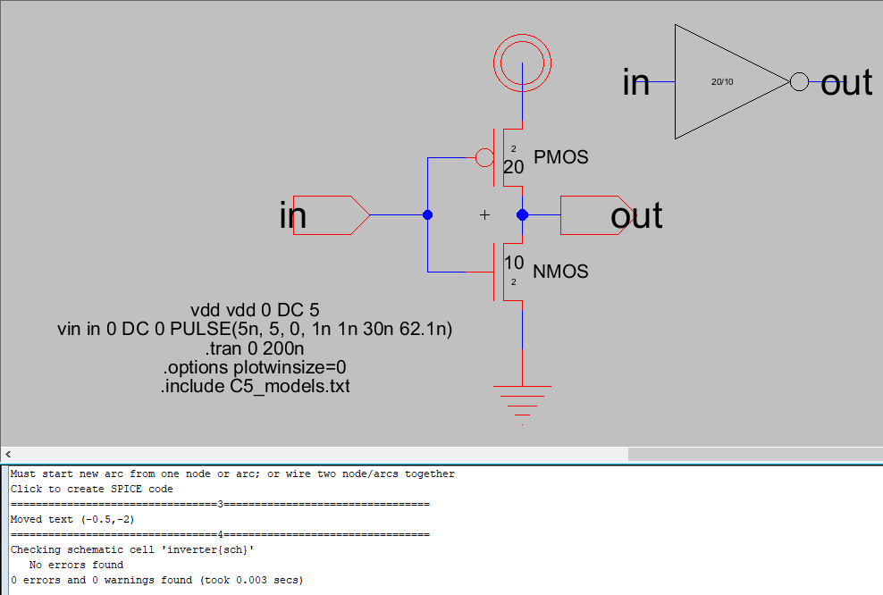
Figure 13. Inverter schematic with the added spice code for the transient analysis using a PULSE function.
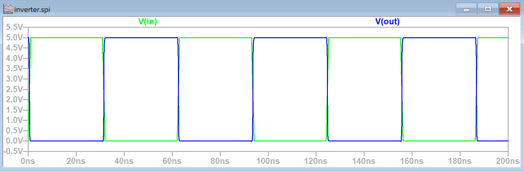
Figure 14. LTSpice simulation plot of V(in) and V(out) when V(in) was defined to be a PULSE function.
Task 2: The layout view of the inverter was successfully created after
following the provided tutorial. The appropriate nodes were added,
widths were adjusted, and the nodes positioned as shown in Figure 15.
The PMOS and NMOS nodes had their spice models set to PMOS and NMOS
respectively. Figure 15 also displays the DRC check results for the
layout view at this point.
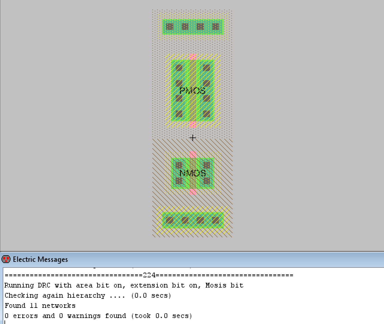
Figure 15. Inverter layout view with the required nodes positioned and sized correctly.
After this the necessary connections were made along with another DRC check.
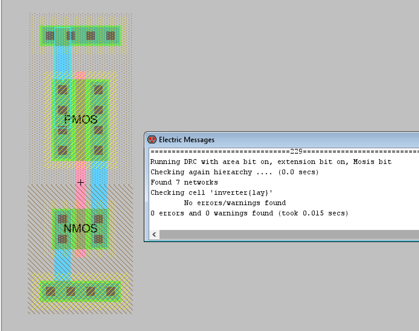
Figure 16. Inverter layout view with the required connections and DRC check results.
After this the metal1 poly contact and the metal1 pin connections were added along with another DRC check.
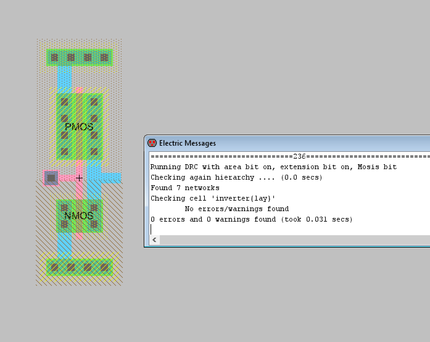
Figure 17. Inverter layout with the metal1 poly contact and the metal1 pin added.
Finally the appropriate pins were exported with the final DRC check for the layout view.
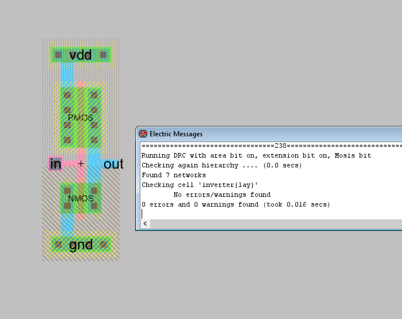
Figure 18. Final inverter layout view with DRC check results.
Task 3: The 100/50 inverter schematic and layout view were successfully
built for task 3. The original inverter created in task 1 was
duplicated and the multiplier function used to set a multiplier of 5 to
the schematic view. Figure 19 shows the schematic view along with the
edited icon view.
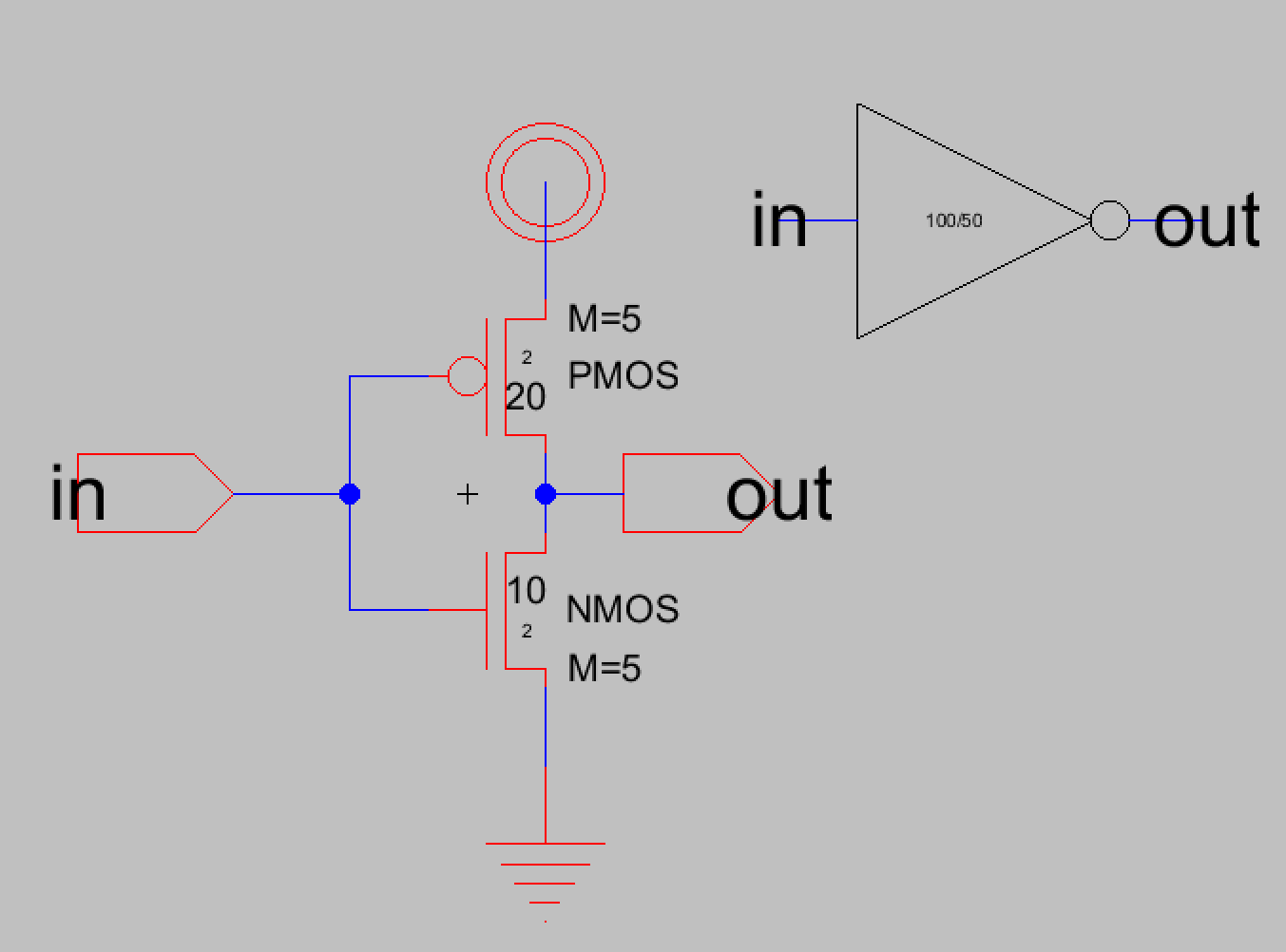
Figure 19. The 100/50 inverter schematic with its icon view displayed.
After this the layout view was edited. The previous connections were
deleted and the PMOS was copied according to the tutorial. Figure 20
shows the first steps for editing the layout view to match the
multiplier schematic along with DRC check results.
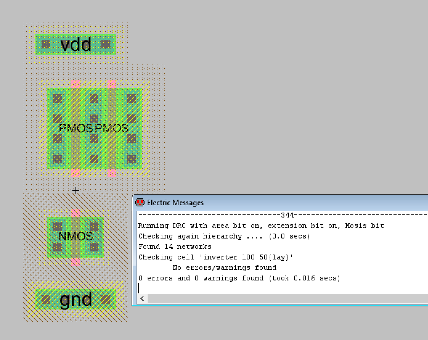
Figure 20. Editing the layout view for the 100/50 inverter. Additional PMOS and NMOS nodes will be added like this.
Now that I had learned how to add the additional PMOS and NMOS nodes I
added more until there were 5 PMOS and 5 NMOS transistors in parallel.
I also edited the VDD and GND nodes to match their width. The
appropriate connections were made according to the tutorial as well.
Figure 21 shows the final layout view for the 100/20 inverter along
with DRC and NCC results.
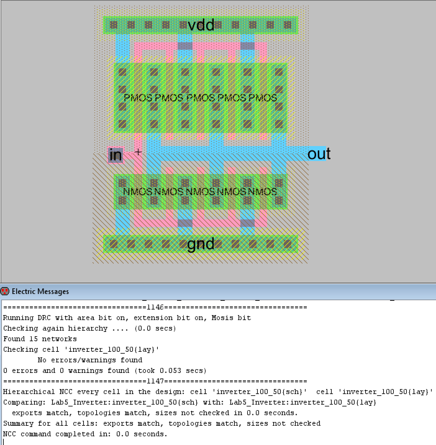
Figure 21. The final layout view for the 100/20 inverter with DRC and NCC check results.
Task 4: I then created the simulation schematic that would simulate the
inverter using spice code. I tested both the 20/10 inverter and the
100/50 inverter with the required 100 fF, 1 pF, and 10 pF load
capacitors and observed their results. The simulation schematics and
LTSpice simulation plots are shown below.
The 20/10 inverter with the 100 fF capacitor had very good inverter
results. The inverted output nearly matches the PULSE function input's
shape.
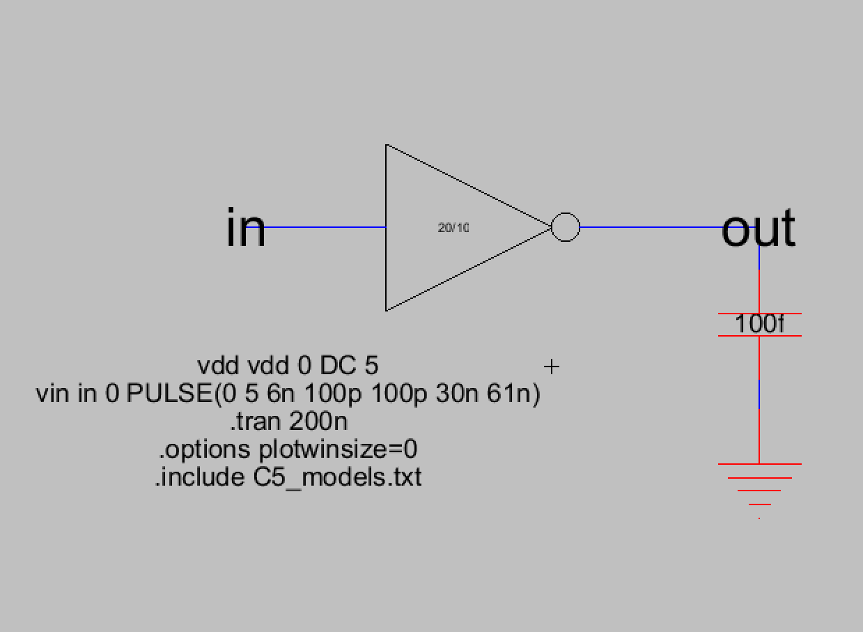
Figure 22. The simulation schematic for the 20/10 inverter with the 100 fF load capacitor.
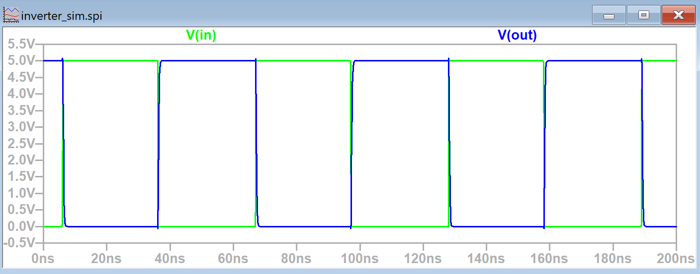
Figure 23. The LTSpice simulation plot of V(in) and V(out) for the 20/10 inverter with 100 fF load capacitor.
The 20/10 inverter with the 1 pF load capacitor displayed more time
delay than with the 100 fF capacitor but was still pretty good.
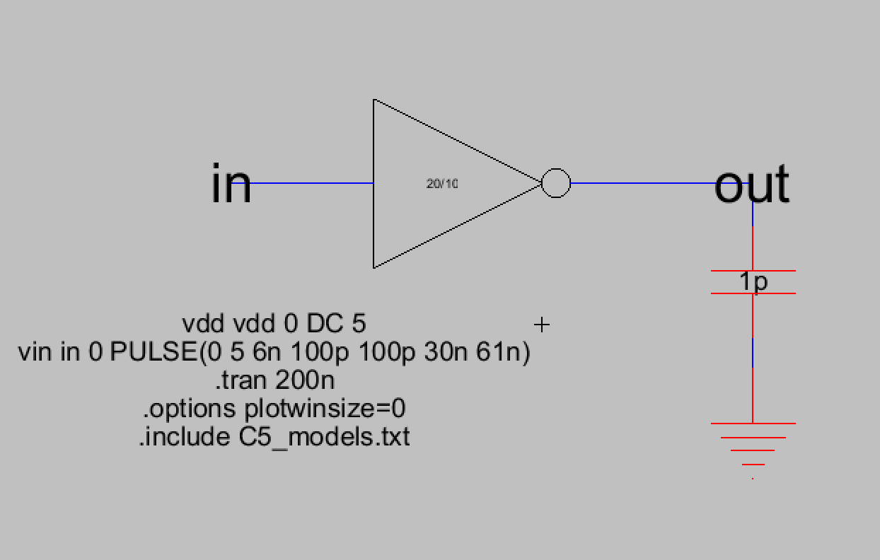
Figure 24. The simulation schematic for the 20/10 inverter with the 1 pF load capacitor.
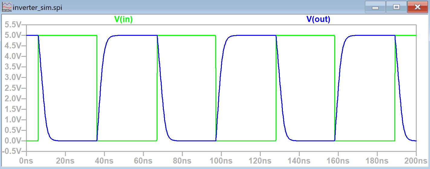
Figure 25. The LTSpice simulation plot of V(in) and V(out) for the 20/10 inverter with 1 pF load capacitor.
The 20/10 inverter with the
10 pF load capacitor had the poorest results out of all the capacitors.
The maximum voltage was never reached due to the time delay.
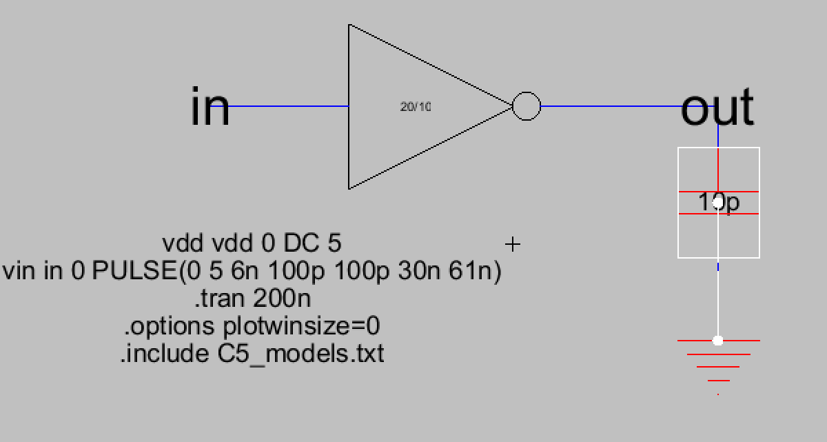
Figure 26. The simulation schematic for the 20/10 inverter with the 10 pF load capacitor.
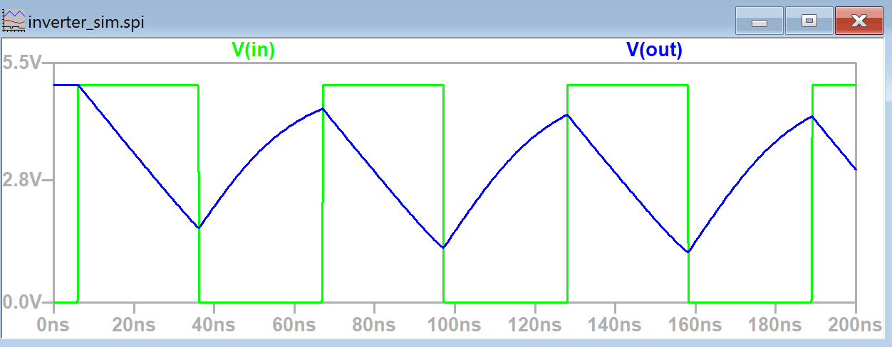
Figure 27. The LTSpice simulation plot of V(in) and V(out) for the 20/10 inverter with 10 pF load capacitor.
Next the 100/50 inverter was simulated using the same three capacitors used for the 20/10 inverter.
When the 100/50 inverter was connected to the 100 fF capacitor the results were similar to the 20/10 inverter.
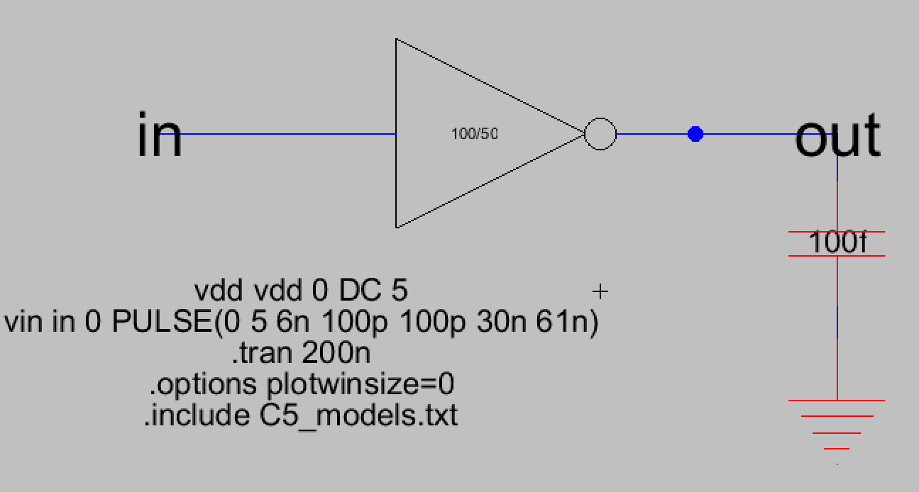
Figure 28. The simulation schematic for the 100/50 inverter with the 100 fF load capacitor.
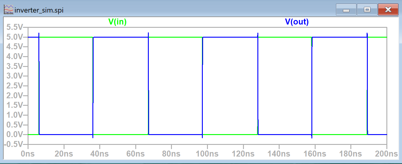
Figure 29. The LTSpice simulation plot of V(in) and V(out) for the 100/50 inverter with the 100 fF load capacitor.
When the 100/50 inverter was connected to the 1 pF capacitor the
results were also more similar to the 100 fF case although there was
still a small time delay. This time delay was much less noticable
however compared to the 20/10 inverter.
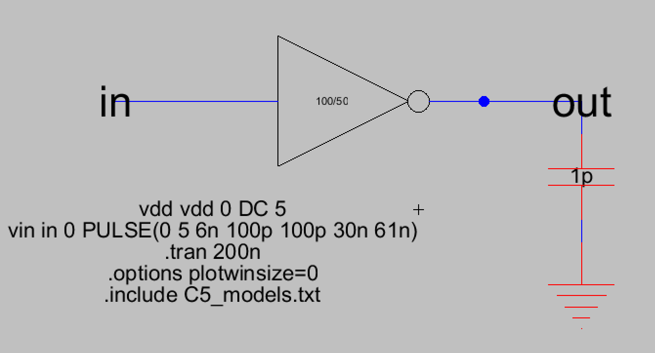
Figure 30. The simulation schematic for the 100/50 inverter with the 1 pF load capacitor.
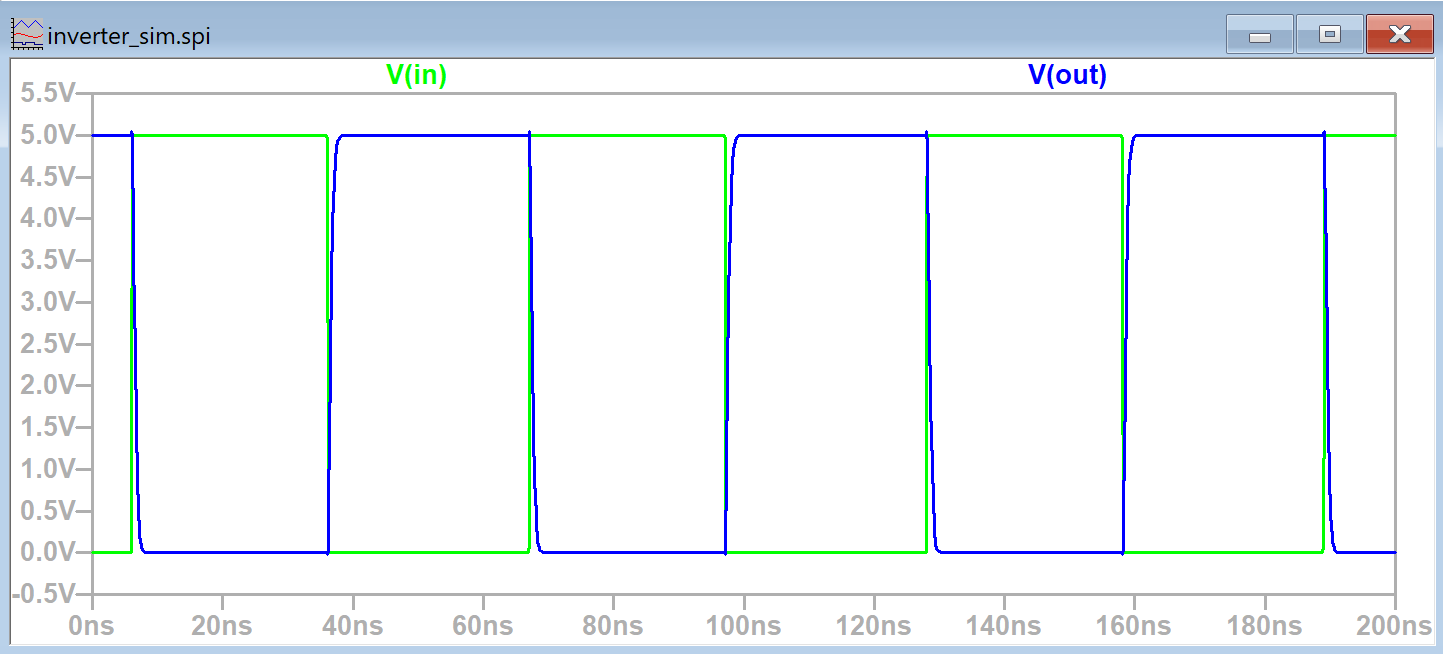
Figure 31. The LTSpice simulation plot of V(in) and V(out) for the 100/50 inverter with the 1 pF load capacitor.
The most noticable improvement was when the 100/50 inverter was used
with the 10 pF load capacitor. The inverter was now able to reach the
peak voltage it wasn't able to reach in the 20/10 inverter case. There
was considerable time delay but the capacitor was now able to charge
all of the way.
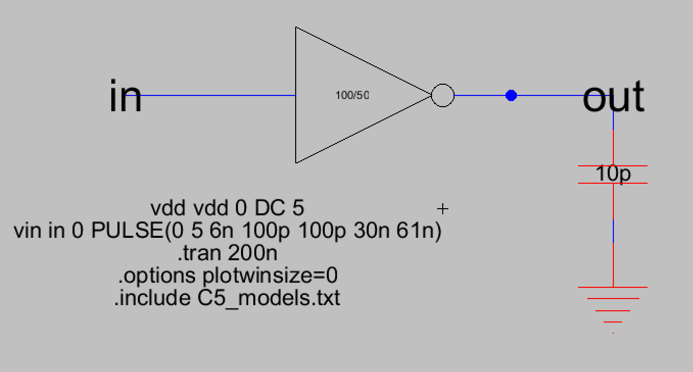
Figure 32. The simulation schematic for the 100/50 inverter with the 10 pF load capacitor.
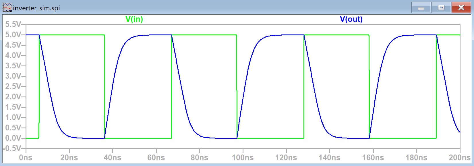
Figure 33. The LTSpice simulation plot of V(in) and V(out) for the 100/50 inverter with the 10 pF load capacitor.
Task 5: The ALS simulation and the IRSIM simulations were
successfully ran for the new inverter simulation schematic shown in
Figure 34. This new simulation schematic contains both the 20/10
inverter and the 100/50 inverter.
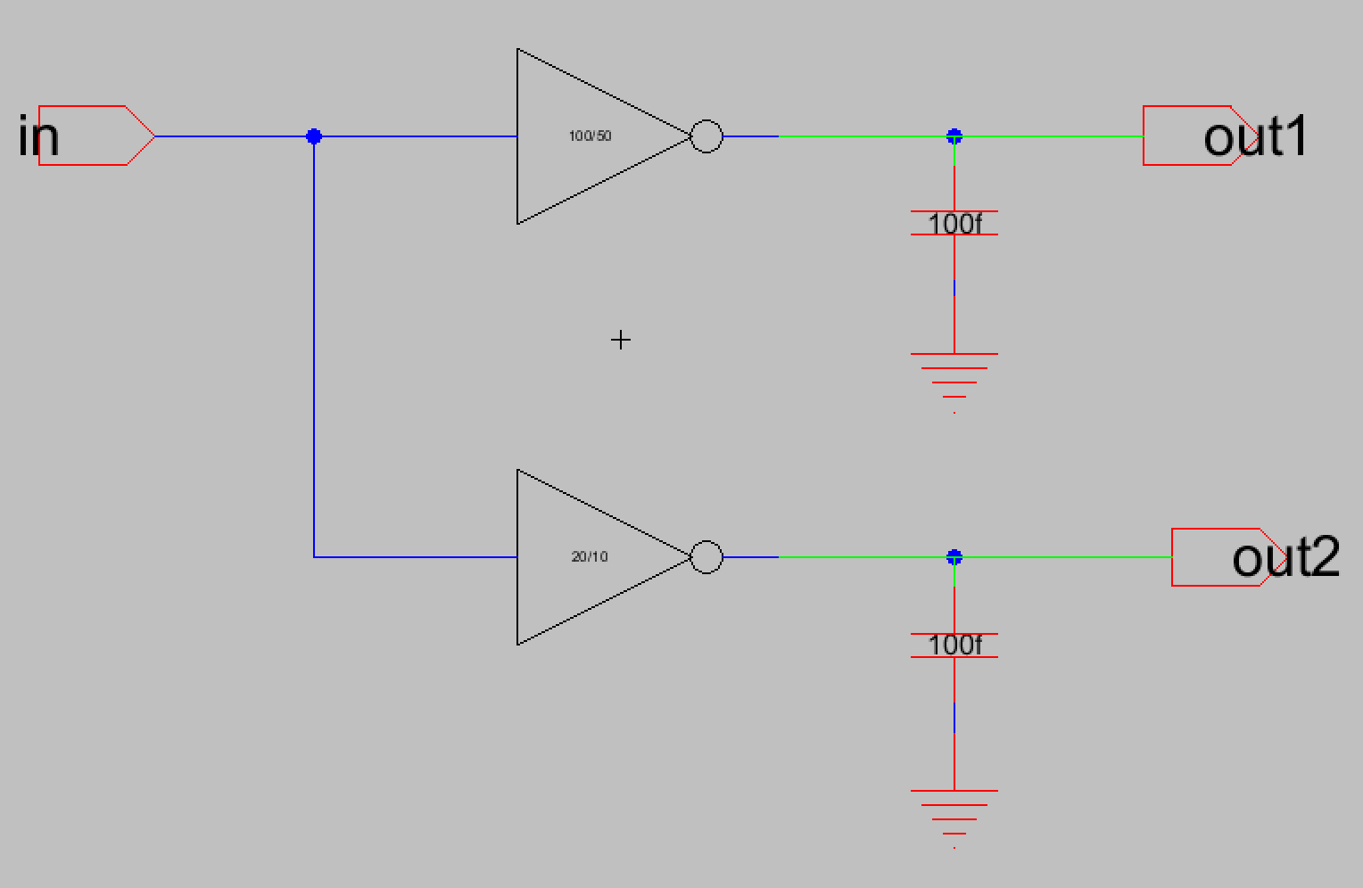
Figure 34. Simulation schematic that contains both the 20/10 inverter with the 100/50 inverter.
The ALS simulation is shown below in Figure 35. The signal for the 'in'
port was successfully edited using the 'v' and 'g' keys to place where
the signal should change from high to low and vice versa.
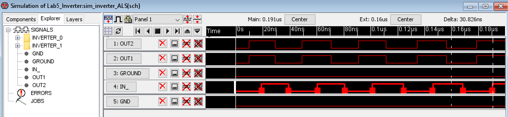
Figure 35. ALS simulation results for the schematic containing both the 20/10 inverter with the 100/50 inverter.
After this the instructions were followed for installing the IRSIM
plugin. The command prompt commands are shown in Figure 36 and the
IRSIM simulation results are shown in Figure 37. The 'in' signal was
edited using 'v' and 'g' keys just like with the ALS simulation.
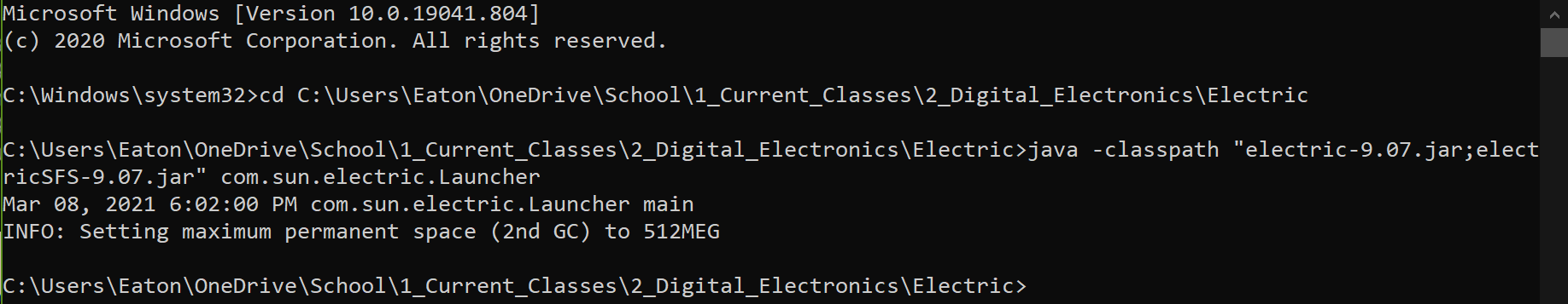
Figure 36. Command prompt commands used to install the IRSIM plugin.
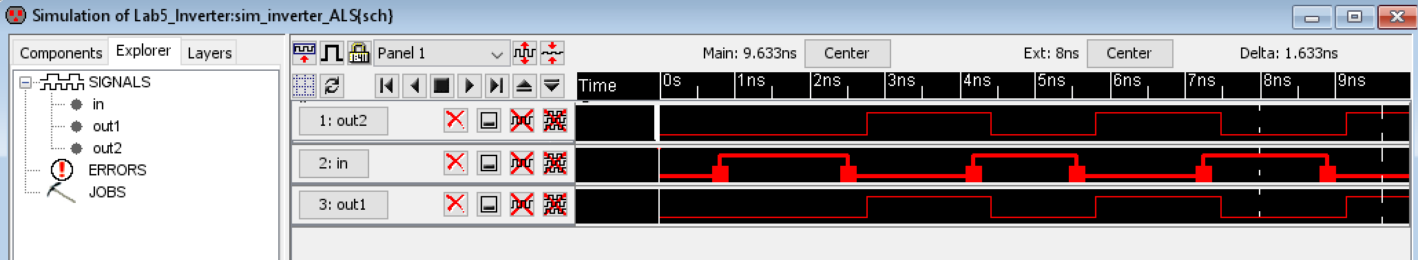
Figure 37. IRSIM simulation results for the schematic containing both the 20/10 inverter with the 100/50 inverter.
Discussion
This lab taught me how the multiplier function can be used in the
schematic view to effectively add multiple copies of a component. I
also learned how the layout view should be modified to match the new
schematic using the multiplier function. One thing I noticed was that
when editing the layout view for the 100/50 inverter, if I changed the
VDD and GND nodes to be 5 times wider then it wouldn't line up with the
rest of the components as was seen in Figure 5. I had to experiment
with the x-size until it was wide enough to match the rest of the
nodes. The correct x-size ended up being 56, not 20*5 or 100 as the lab
instructions said. It may have been my spacing between the various
nodes, which was 4.5, but I don't think that was the cause since it
wouldn't add up to a difference of nearly 50 units. It was also cool to
see the different simulators we hadn't used before. I was curious about
them since I had seen them whenever LTSpice simulations were used in
Electric VLSI and I think its pretty cool that the signal can be
modified manually.