ENGR338 Lab 2021
Spring
Lab 4 MOSFETs and IV Curves
Name: Sean
Eaton
Email:
smeaton@fortlewis.edu
MOSFETS and IV Curves
Introduction
In this lab we were tasked with building MOSFETs in Electric VLSI. The
major parts of this lab were creating the 4 port NMOS and PMOS
schematics, their layouts, and then simulating the designs to analyse
the IV curves of them. The majority of the tutorial was also created by
Dr. R. Jacob Baker who was our professor's PHD adviser at the
University of Las Vegas (UNLV).
NMOS
IV:
When
creating the NMOS IV schematic we first added a NMOS transistor and
modified the width and length to be 10 and 2 respectively. Then the
spice model was added and the text was changed to NMOS, rotated to be
horizontal, and rearranged to resemble the schematic seen below in
Figure 1. This was repeated for the PMOS schematic which should like
Figure 2 below.
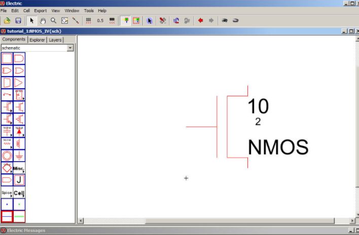
Figure 1. The
initial NMOS IV schematic.
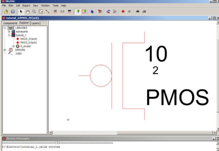
Figure 2. The
initial PMOS IV schematic.
After
doing this the NMOS and PMOS nodes should be changed to be a 4-Port
Transistor node via the following menu options seen in Figure 3.
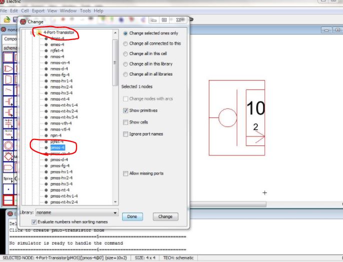
Figure 3.
Changing the PMOS node to be a 4-Port Transistor Node.
Next
the layout view should be created. For the NMOS layout the NMOS node
was added, as well as 2 nAct nodes, a metal1 contact node, and a pWell
node. The NMOS node should also have its spice model set to be NMOS as
well. All the nodes with the added spice model should look similar to
Figure 4 below.
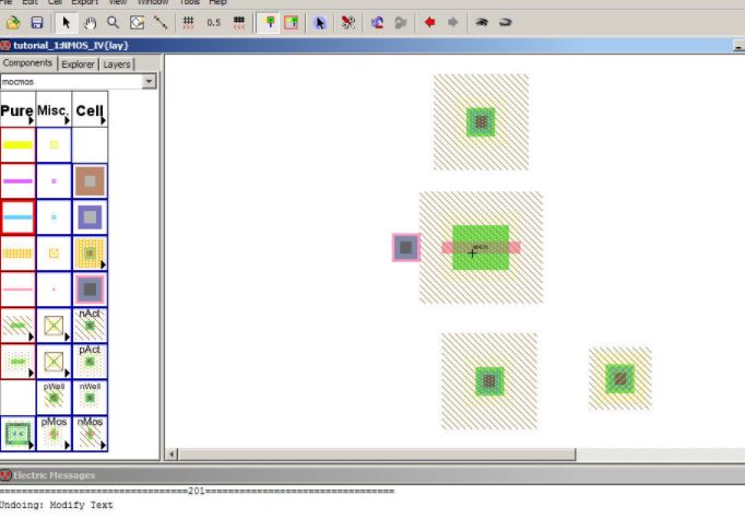
Figure 5. All
required nodes in the layout view with the NMOS node's spice model set
to NMOS.
The
nodes have to have their properties edited so that their x-sizes are
all 10 to be consistent with the schematic. The metal1 node does not
have to have its x-size adjusted. The modified x-sizes are shown below
in Figure 6.
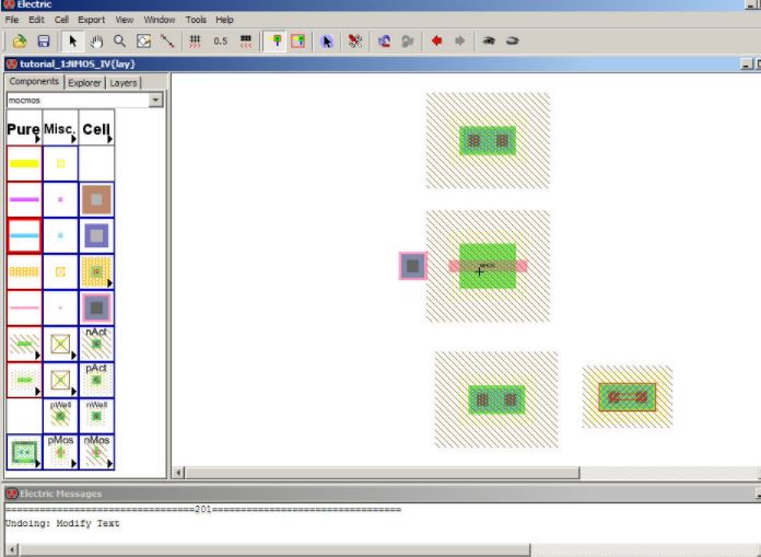
Figure 6. Edited
nodes that have their x-size set to 10.
N-Active
Arcs should be added to connect the NMOS node to the nAct above as
shown below. This first added arc should be added from the NMOS node to
the above nAct node and not the other way around.
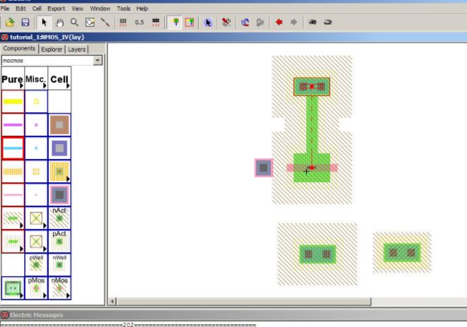
Figure 7.
Connecting the first N-Active Arc from the NMOS node to the nAct node
above.
The
nAct node can then be moved down until it connects to the NMOS node as
seen in Figure 8. The next N-Active Arc can be connected from the nAct
node below to the NMOS node (reversing the order seen above) but the
N-Active Arc will look like the one seen in Figure 8.
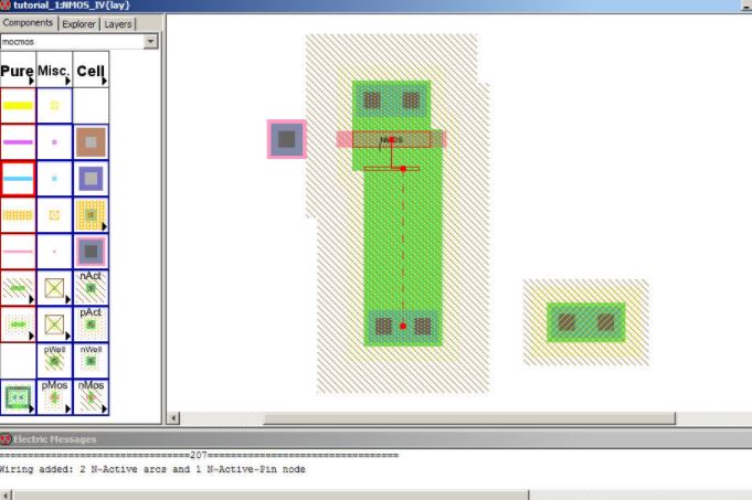
Figure 8. The
top nAct node has been moved closed to the NMOS node. The bottom nAct
node has its N-Active Arc misaligned.
The
misaligned N-Active Arc can be fixed by editing its properties to make
the arc rigid. There is also an issue with the Arc extending beyond the
poly1 area (pink section). Select the N-Active Arc and align it with
the NMOS node. The nAct node should move along with it as seen below.
Move the nAct node up to the NMOS node like with the top nAct node.
There should be 5 DRC errors which can be fixed by editing the Arc's
properties to set the End Extension to be "Neither End". After doing
this the layout view should look like the one shown in Figure 9.
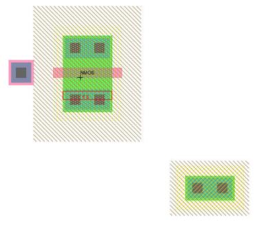
Figure 9. The
bottom nAct node has been positioned correctly with no DRC errors.
The
metal1 contact should now be connected to the left poly1 port of the
NMOS node. There should be no DRC errors if it is done correctly. A
well check can be confirmed and should result in an error since the
p-well node is not connected to ground. The p-well should be moved over
so that it connects up with the NMOS p-well layer as seen below in
Figure 10. An ERC check should result in a single error.
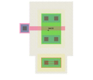
Figure 10. The
metal1 contact connected to the left poly1 port with the p-well
connected to the p-well layer.
Arcs
should then be added for the drain, gate, source, and ground
connections. Their pins should be exported to d, g, s, and gnd as seen
below in Figure 11. After this is done the layout view should pass DRC
and ERC-Check Wells.
Figure 11.
Layout view with the appropriate arcs and pins exported.
PMOS IV:
A
similar process should be carried out for the PMOS IV layout. The
following nodes should be added to the PMOS IV layout, nWell, 2x pAct,
PMOS, and metal1-poly contact as seen in Figure 12.
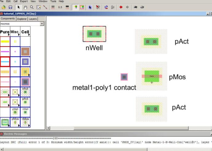
Figure 12.
Required nodes for PMOS IV layout.
The
nWell node needs to be adjusted to have a y-size of 6 to avoid errors.
All of the nodes except for the metal1 node should also have their
x-size adjusted to 10. Everything should be connected together
similarly to the NMOS IV schematic, the result is seen below in Figure
13.
Figure
13. PMOS IV layout view with all connections made.
IV Curves:
Now
that the layout view has been completed, spice code should be added to
the layout view to see the simulation results. The spice code for the
NMOS IV and PMOS IV is seen below:
NMOS IV Spice Code:
vs s 0 DC
0
vw w
0 DC 0
vg g 0 DC
0
vd d 0 DC
0
.dc vd 0
5 1m vg 0 5 1
.include
C:\Electric\C5_models.txt
PMOS IV Spice Code:
vs s 0 DC
0
vw w 0 DC
0
vg g 0 DC
0
vd d 0 DC
0
.dc vd 0
-5 -1m vg 0 -5 -1
.include
C:\Electric\C5_models.txt
It
should be verified that the Write Spice Deck function works and the IV
Curves for the NMOS IV and PMOS IV can be plotted. This is done by
adding the trace Is(Mnmos@0) and Is(Mpmos@0) respectively. The IV curve
should look similar to those shown in Figures 14 and 15 below.
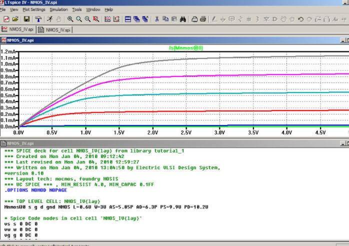
Figure 14. IV
curve for the NMOS IV layout.
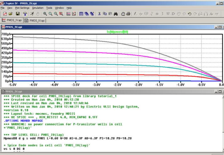
Figure 15. IV
curve for the PMOS IV layout.
Now
the schematic view for the NMOS IV and PMOS IV should be edited just
like the layout view. Arcs should be added and the pins exported to
match the layout view's exported pins. For the NMOS IV a ground pin
should also be added. The same spice code should be added and the IV
curves should be verified. An NCC check should be ran to verify that
the schematic matches the layout view. The final NMOS IV and PMOS IV
schematics are seen below in Figures 16 and 17.
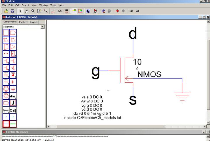
Figure 16. The
finished NMOS IV schematic.
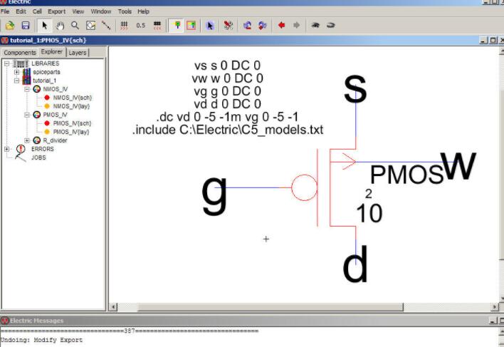
Figure 17. The
finished PMOS IV schematic.
Results
The
NMOS IV and PMOS IV schematic were successfully created. The width was
changed to 10 and the labels were appropriately rotated and positioned
as seen in Figures 18 and 19 below.
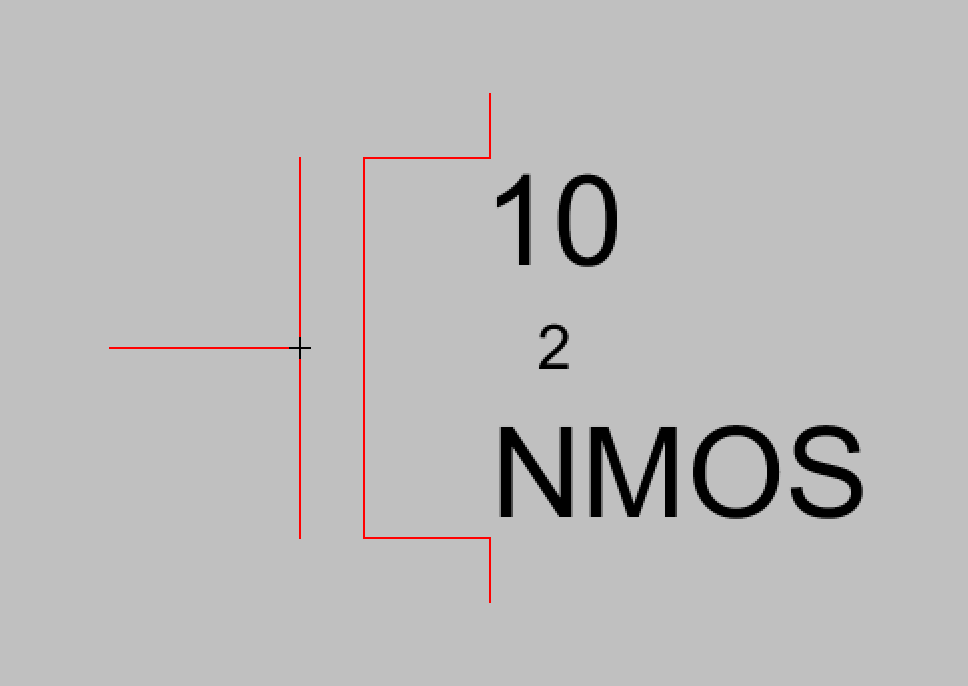
Figure 18.
Initial NMOS IV schematic.
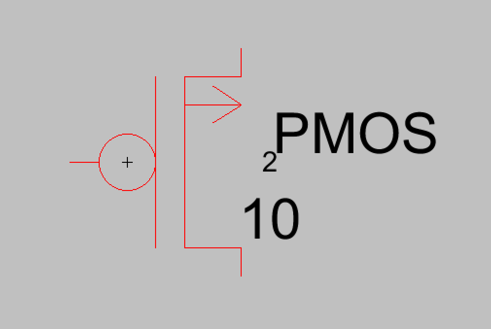
Figure 19.
Initial PMOS IV schematic.
In the layout view, the necessary nodes for the NMOS IV were added as
seen in Figure 20.
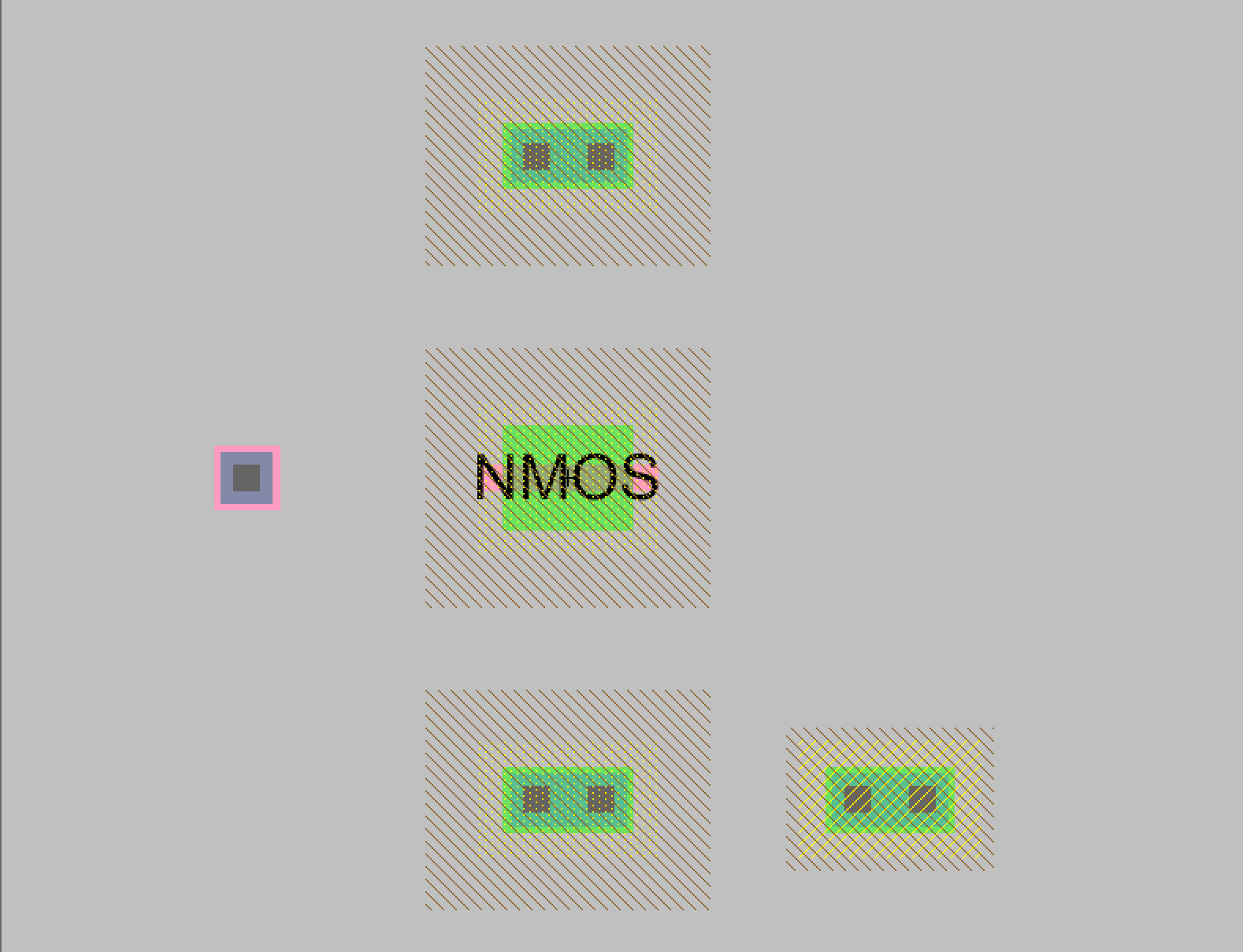
Figure 20. NMOS
IV nodes added to the layout view.
After
connecting the top nAct node to the NMOS node a DRC check was performed
to verify no errors. The results are seen in Figure 21. The nAct node
was moved closer to the NMOS node as well.
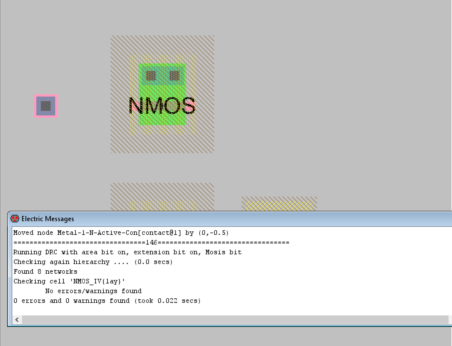
Figure 21. Post
connecting the above nAct node to the NMOS node.
The
bottom nAct node was connected according to the tutorial but the
results were not the same. The N-Active Arc did not behave the same as
in the tutorial. This is shown in Figure 22.
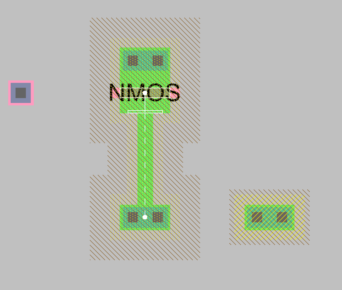
Figure 22.
Connecting the bottom nAct node to the NMOS node. The N-Active Arc
behaved like the top N-Active Arc.
Since
the N-Active Arc behaved like the top nAct node's N-Active Arc it was
left alone. The bottom nAct node was moved closer and a DRC check was
performed. The results were good as shown in Figure 23.
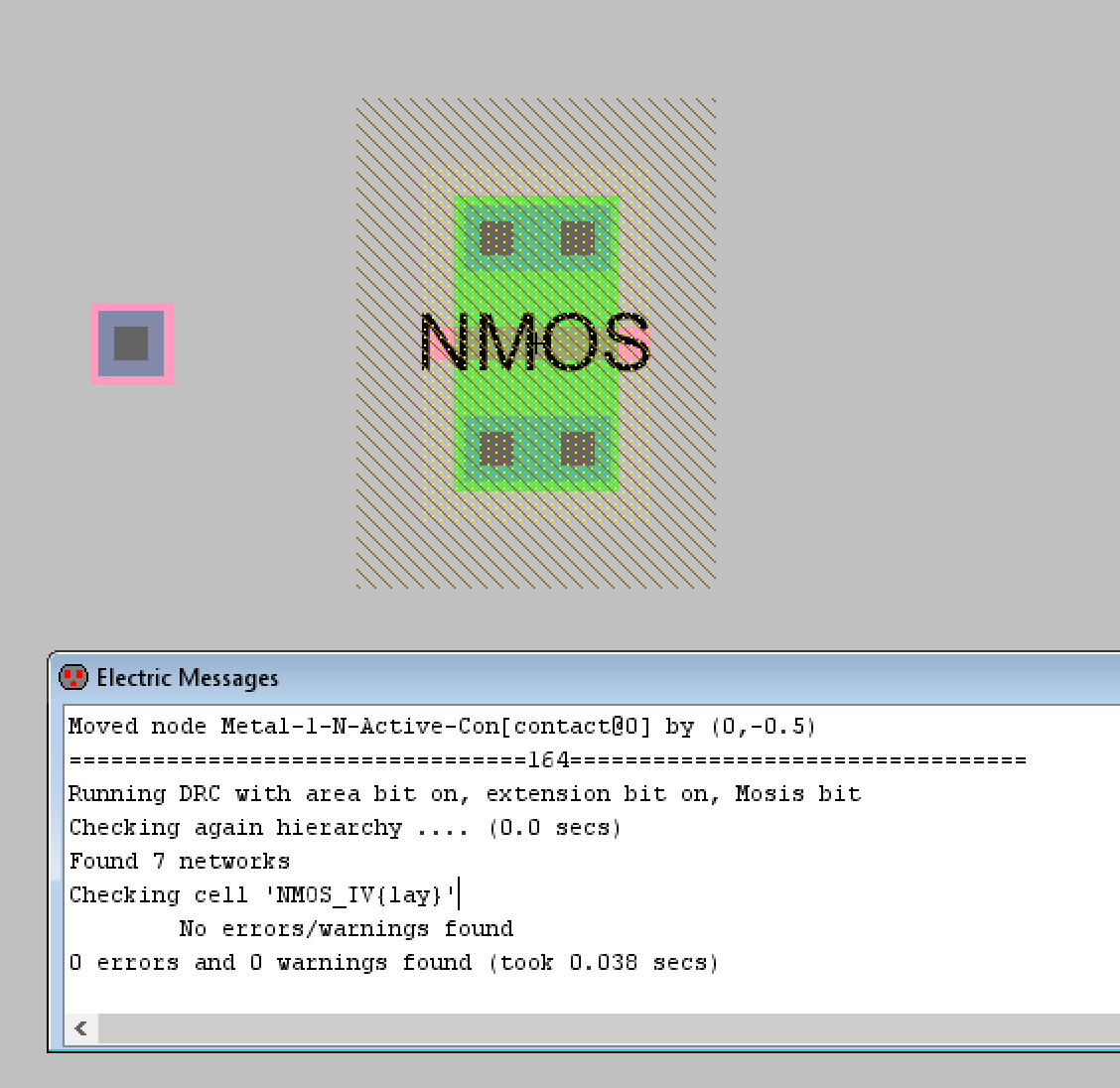
Figure 23.
Moving the nAct node up to the NMOS node with DRC check results.
The metal1 contact was then connected to the left poly1 port. The DRC
check performed also passed.
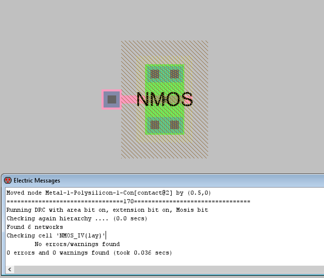
Figure 24. DRC
check results after connecting metal1 to the left poly1 port.
The ERC Well check was then performed which found 2 well errors as
expected. The results are shown in Figure 25.
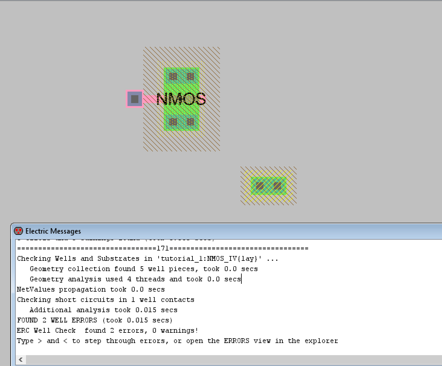
Figure 25. ERC
Well Check results for the NMOS IV layout view.
The
p-well node was moved closer as instructed. The ground arc was added
for the p-well and the pin exported as well. This resulted in no ERC
well check errors as shown in Figure 26.
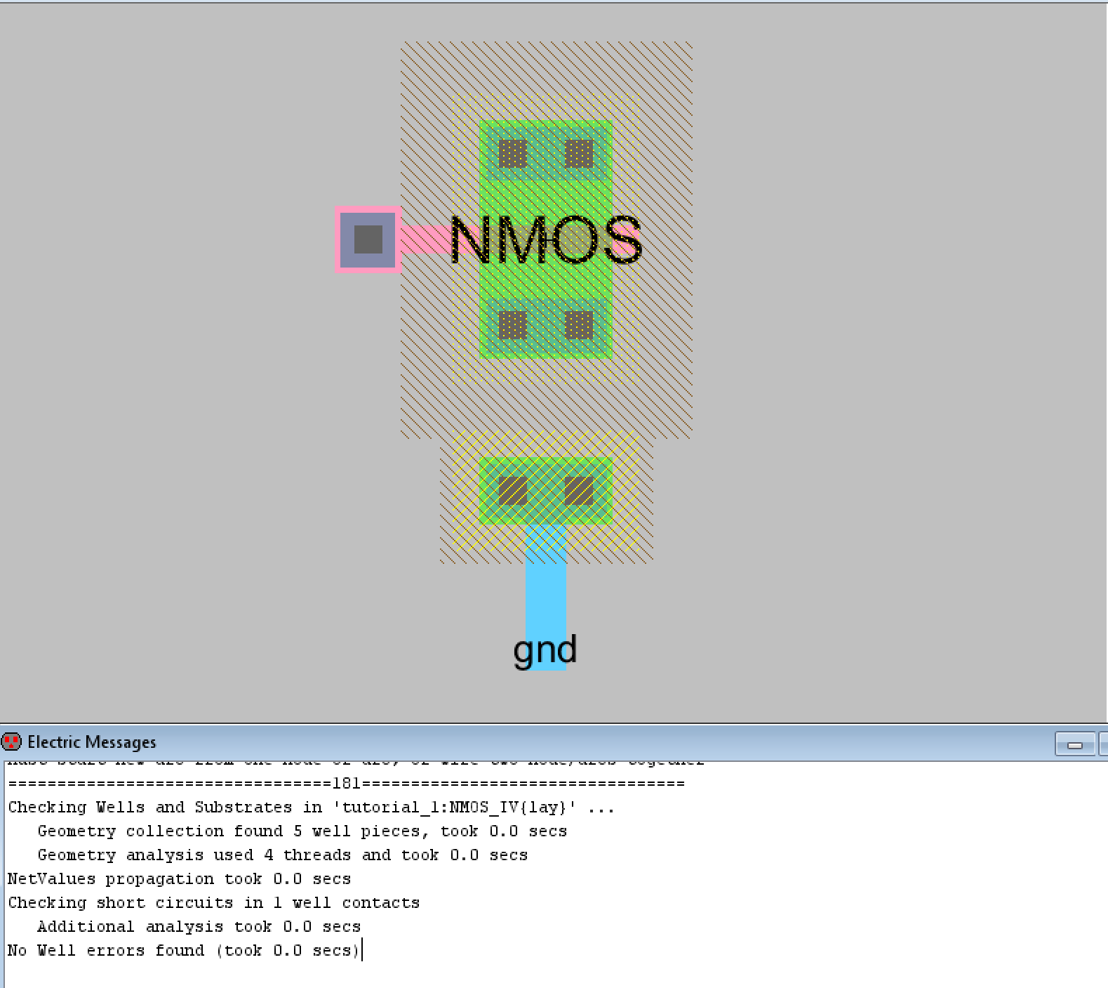
Figure 26. ERC
Well Check results after moving the p-well node closer and exporting
the ground pin.
After this the appropriate source, drain, and gate pins were exported
as shown in Figure 27.
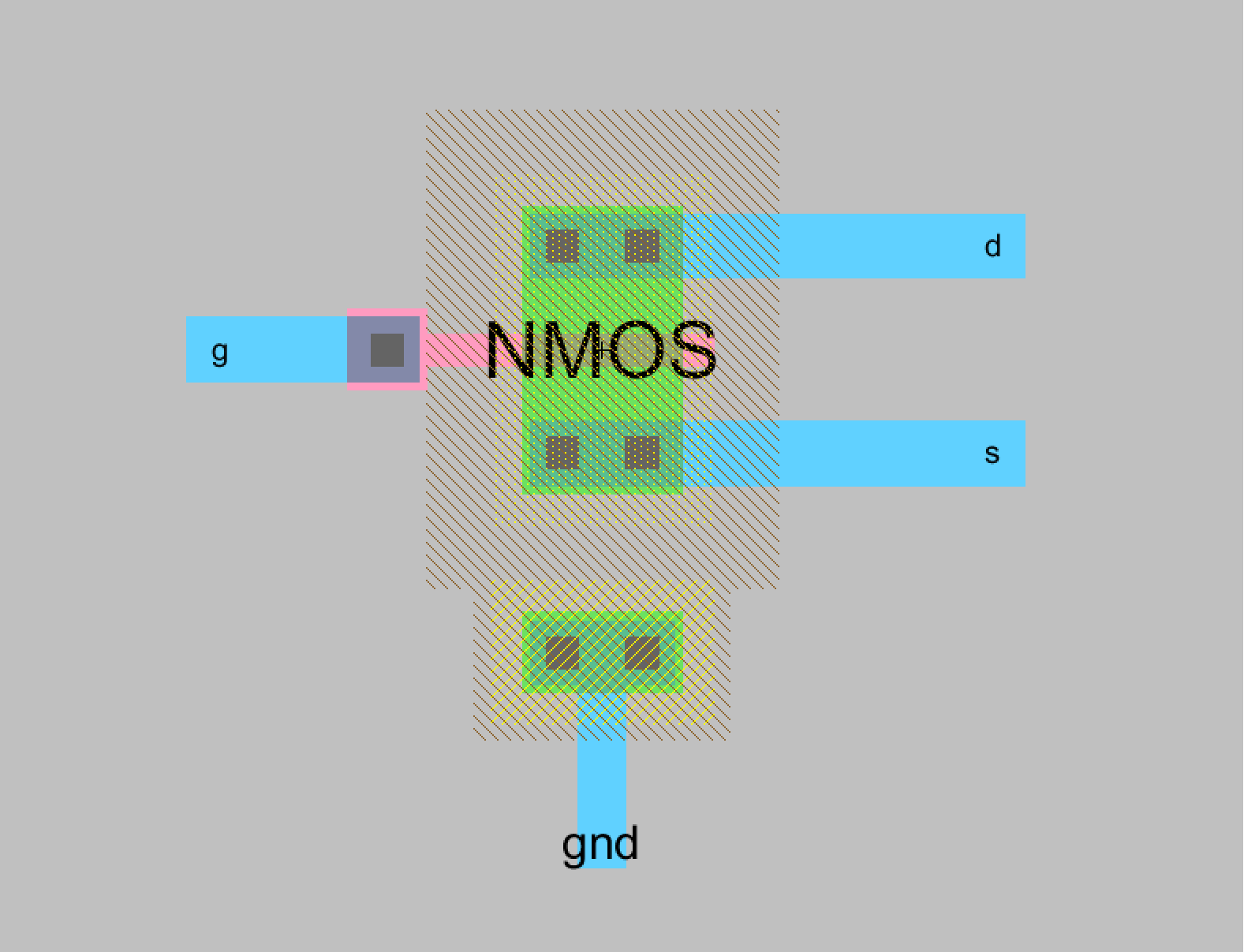
Figure 27. The
NMOS IV layout with the d, g, s, and gnd pins exported.
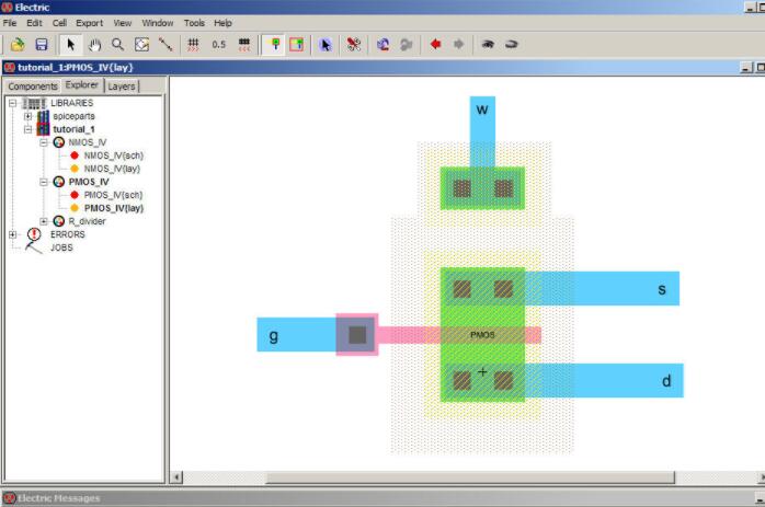
For the PMOS IV layout, the necessary nodes were added as shown in
Figure 28.
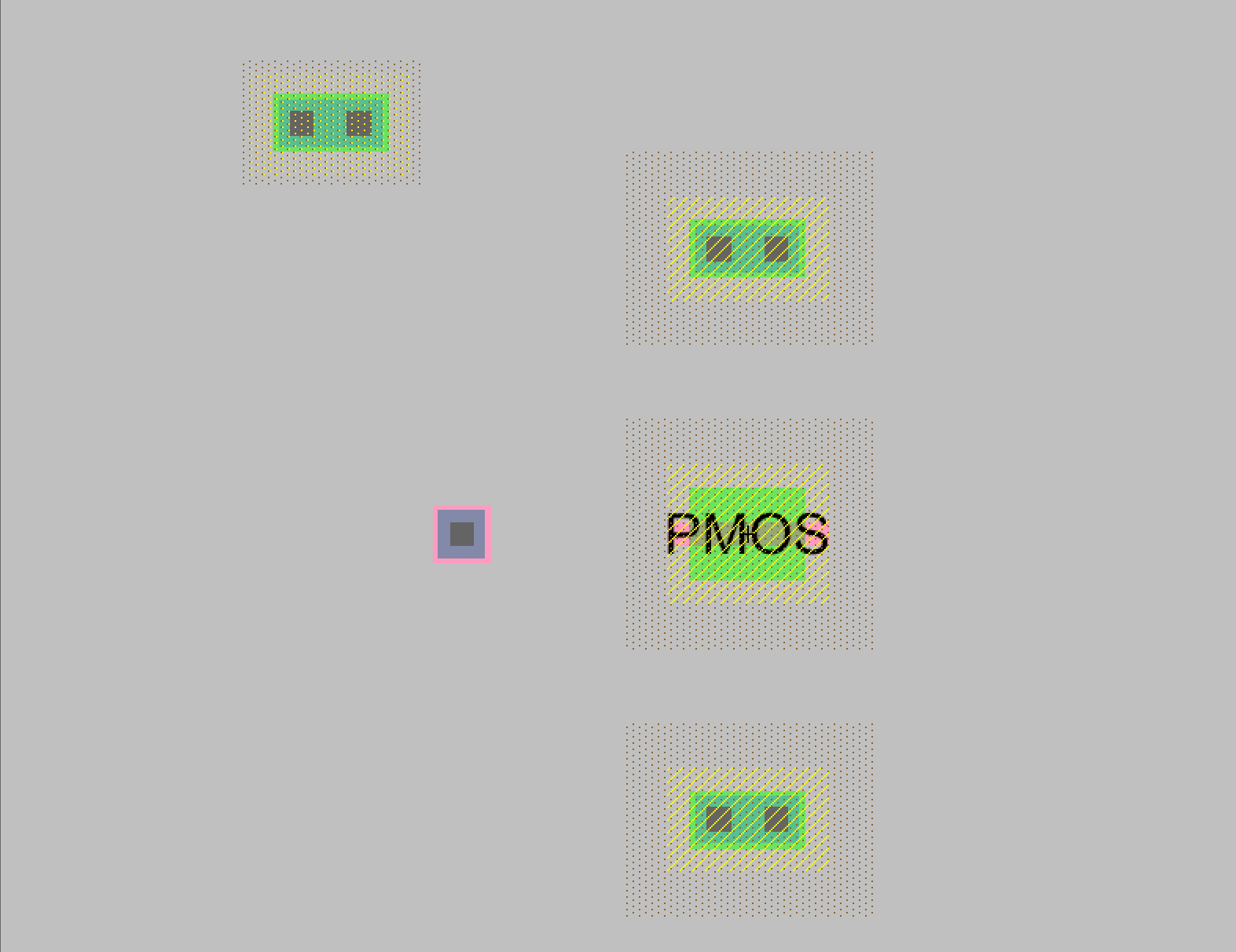
Figure 28. The
PMOS IV layout with the necessary nWell, 2x pAct, pMOS, and
metal1-poly1 contact nodes.
The
nodes were connected together and positiona appropriately with the pins
exported. The DRC check passed successfully and the results are shown
in Figure 29.
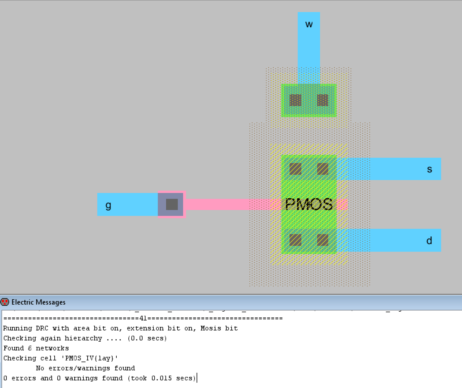
Figure 29. DRC
Check results for the connected PMOS IV layout.
An ERC well check was also performed with no errors being found as
shown in Figure 30.
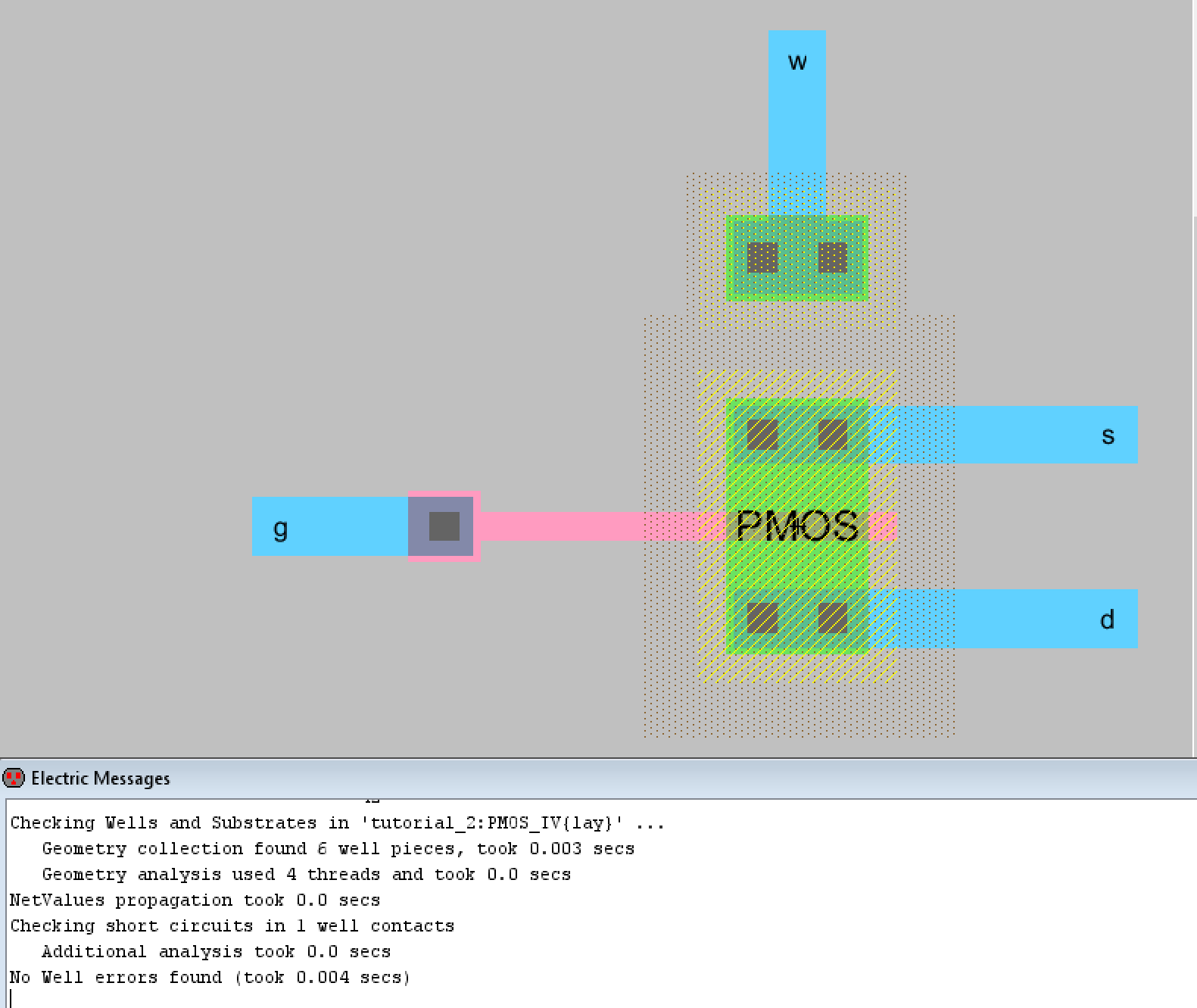
Figure 30. ERC
Well Check results for the connected PMOS IV layout.
After
this the relevant spice code was added for the PMOS IV layout as shown
in Figure 31. The results matched what was expected although the
LTSpice wouldn't allow the x-axis to begin from -5V so the plot looks
flipped as seen in Figure 32.
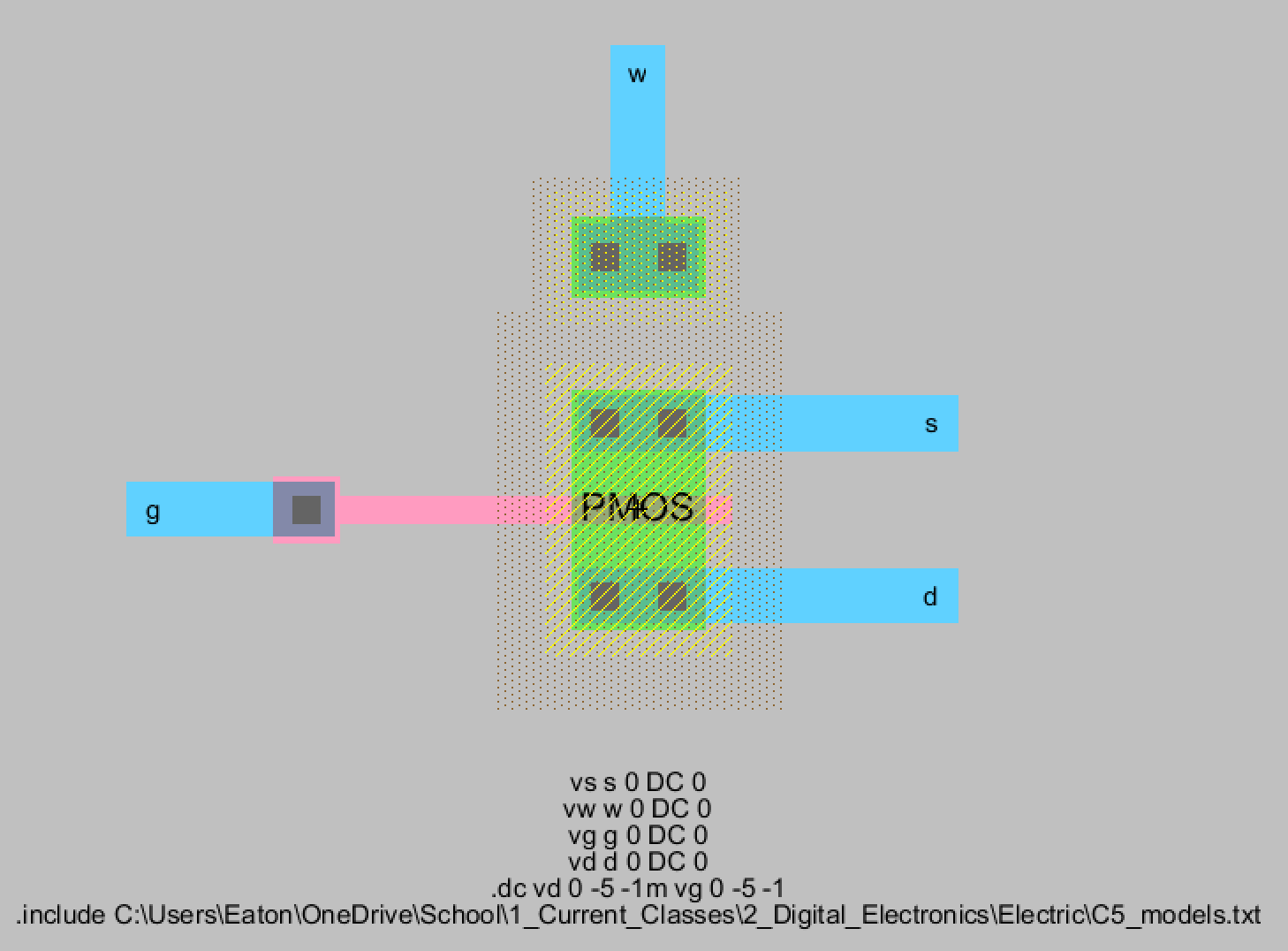
Figure 31. The
PMOS IV layout with the added Spice code.
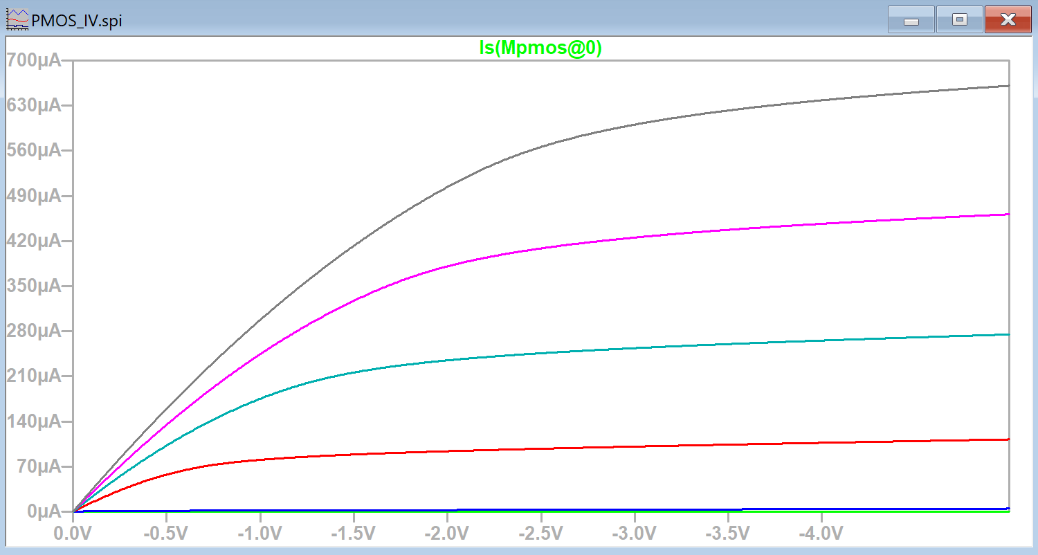
Figure 32. PMOS
IV layout's IV curve.
For
the NMOS IV layout this process was repeated with the appropriate spice
code as seen in Figure 33. Figure 34 shows the simulation plotting
results which are consistent with the expected results.
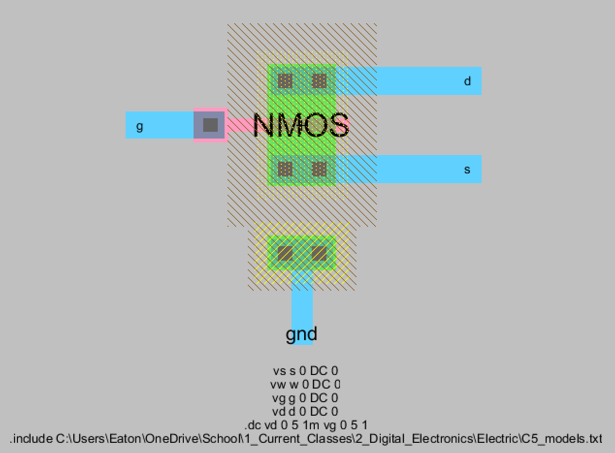
Figure 33. NMOS
IV layout with the added Spice code.
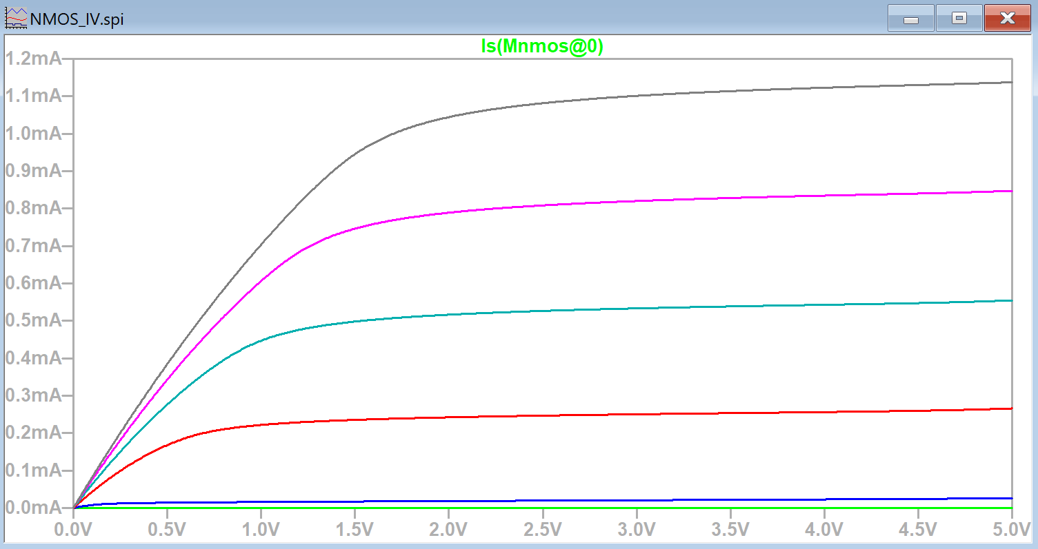
Figure 34. NMOS
IV layout's IV curve.
The spice code was also added to the NMOS IV schematic and the PMOS IV
schematic as seen in Figures 35 and 36.

Figure 35. Added
spice code to the NMOS IV schematic.
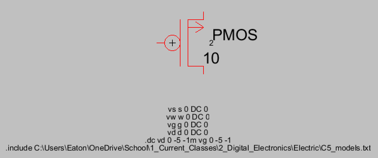
Figure 36. Added
spice code to the PMOS IV schematic.
For
the NMOS IV schematic the appropriate pins were exported and a
connection to ground was added. An NCC check was performed and passed
as shown in Figure 37. Boxes were also added to match the tutorial. The
simulation plotting results are shown in Figure 38.
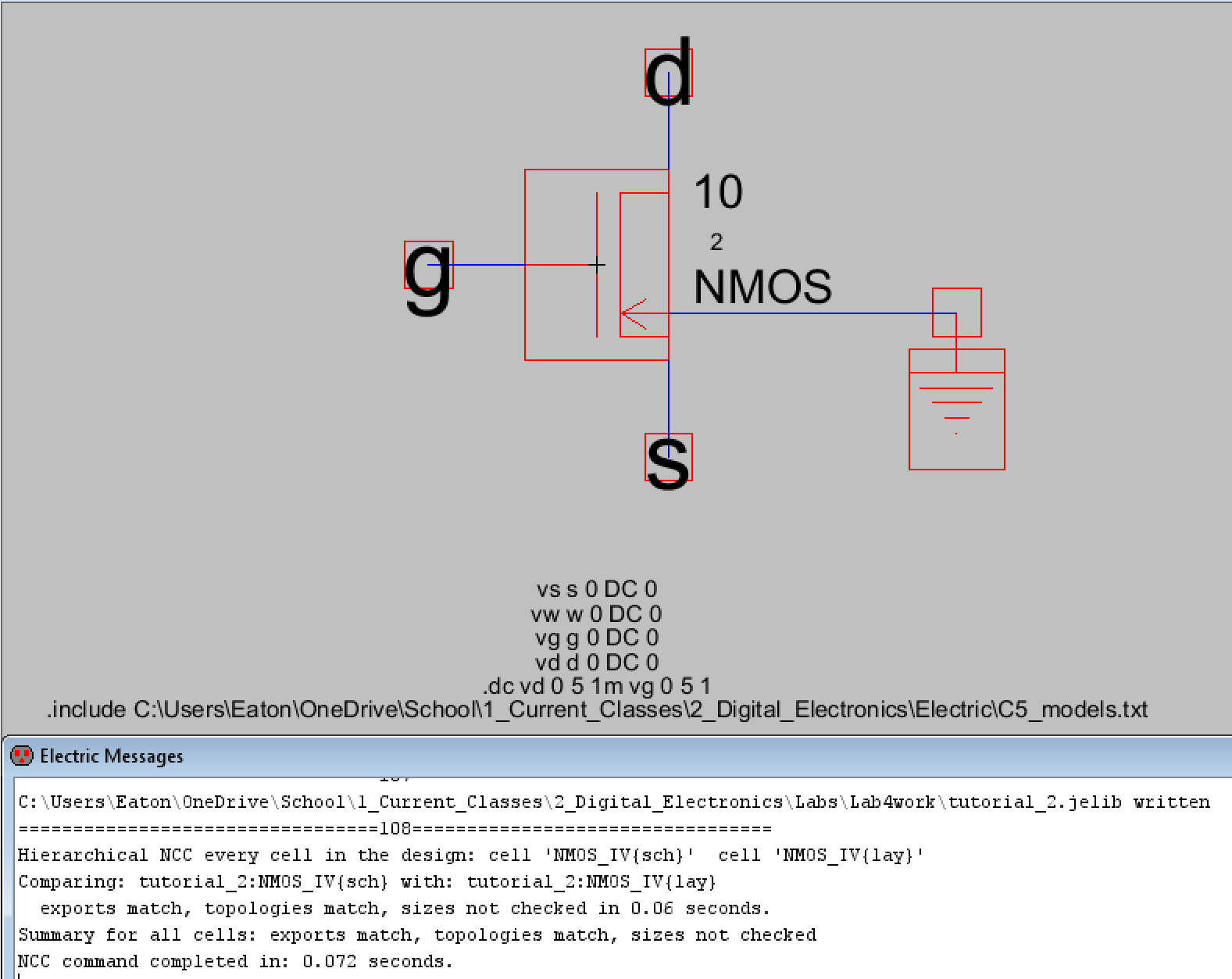
Figure 37. NCC
Check results for the final NMOS IV schematic.
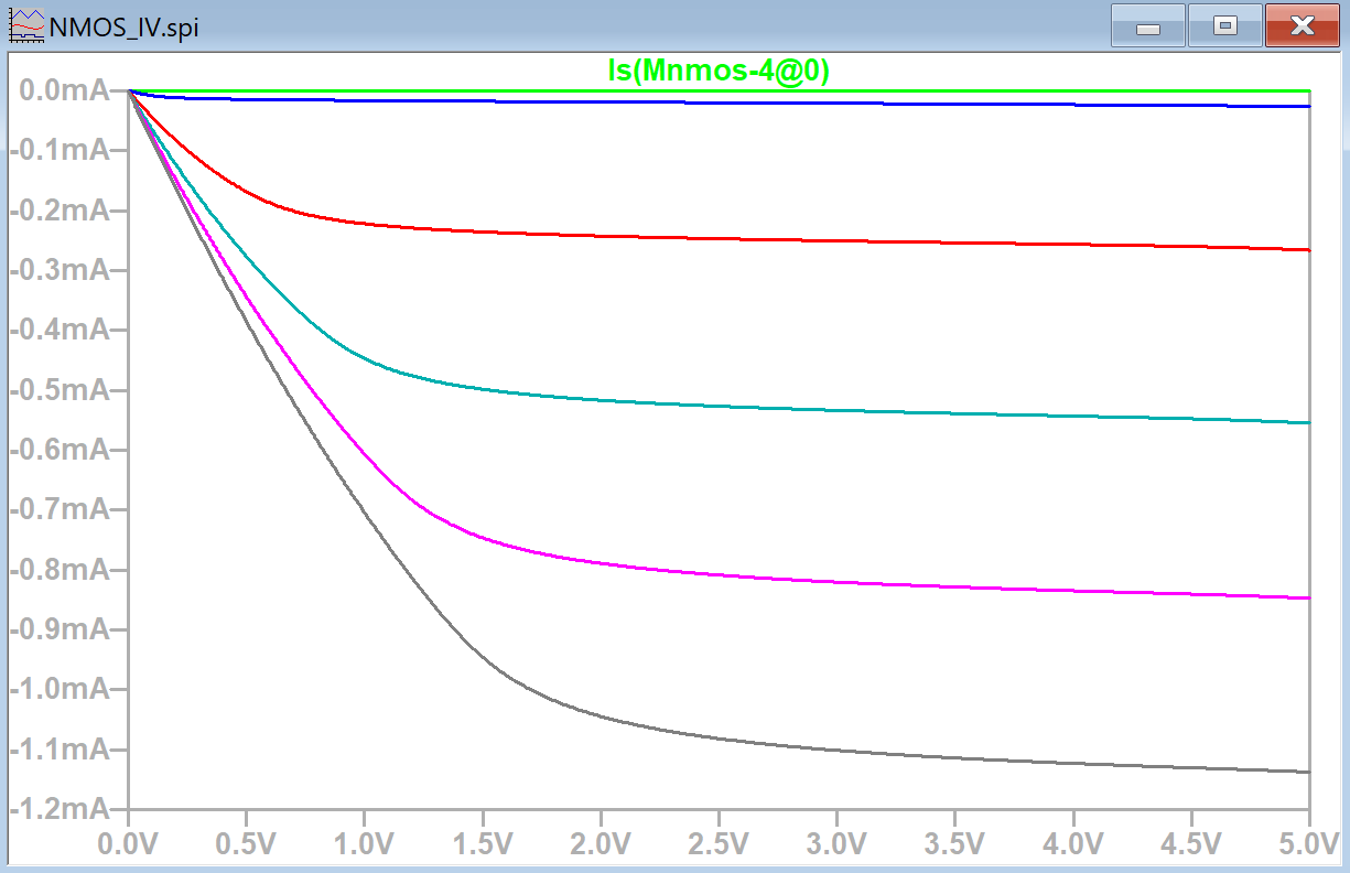
Figure 38. The
LTSpice simulation plot for the final NMOS IV schematic.
For
the PMOS IV schematic the appropriate pins were added and exported.
Another NCC check was performed and passed with the results shown in
Figure 39, Figure 40 shows the LTSpice simulation's results plotted.
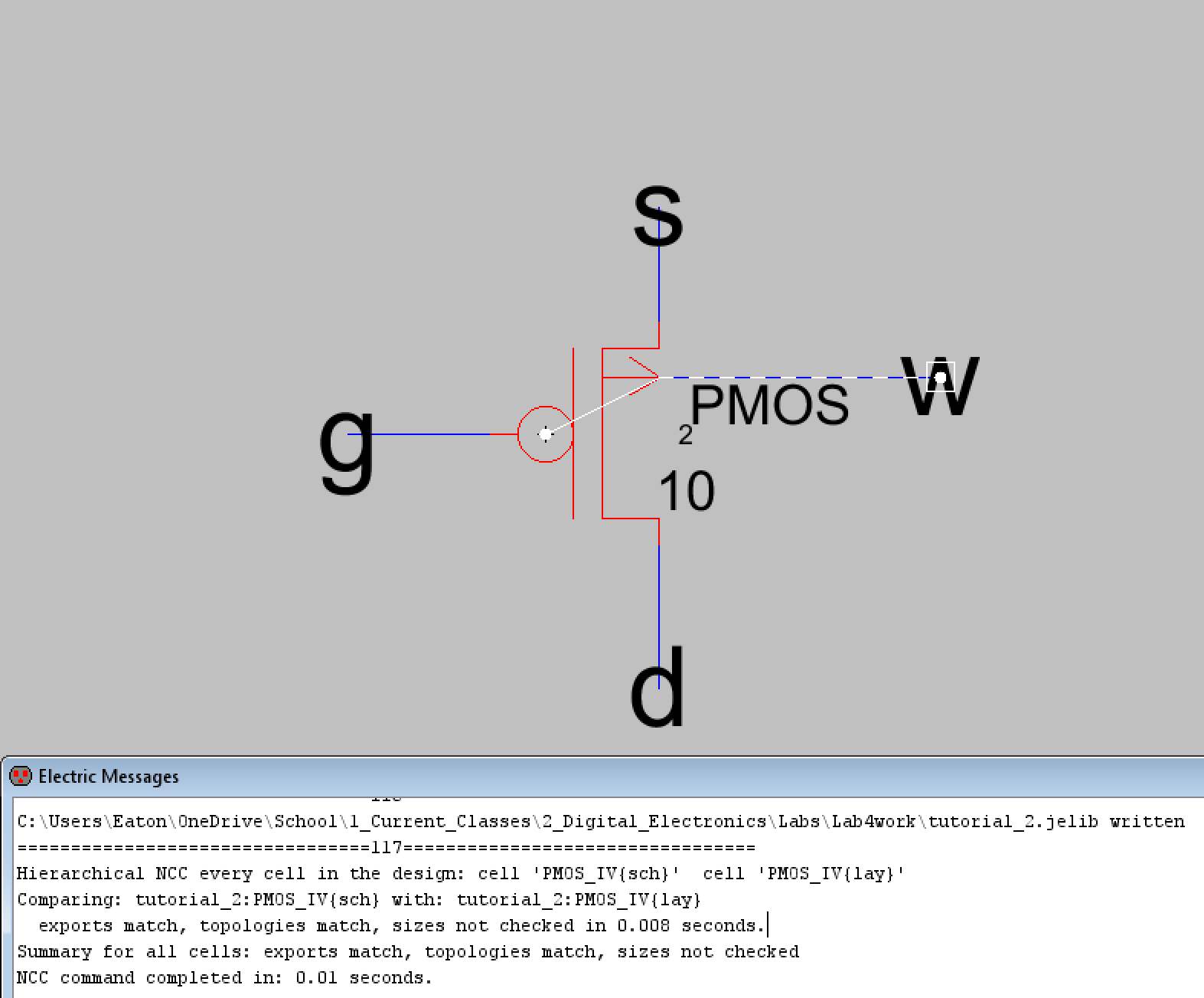
Figure 39. NCC
results for the final PMOS IV schematic.
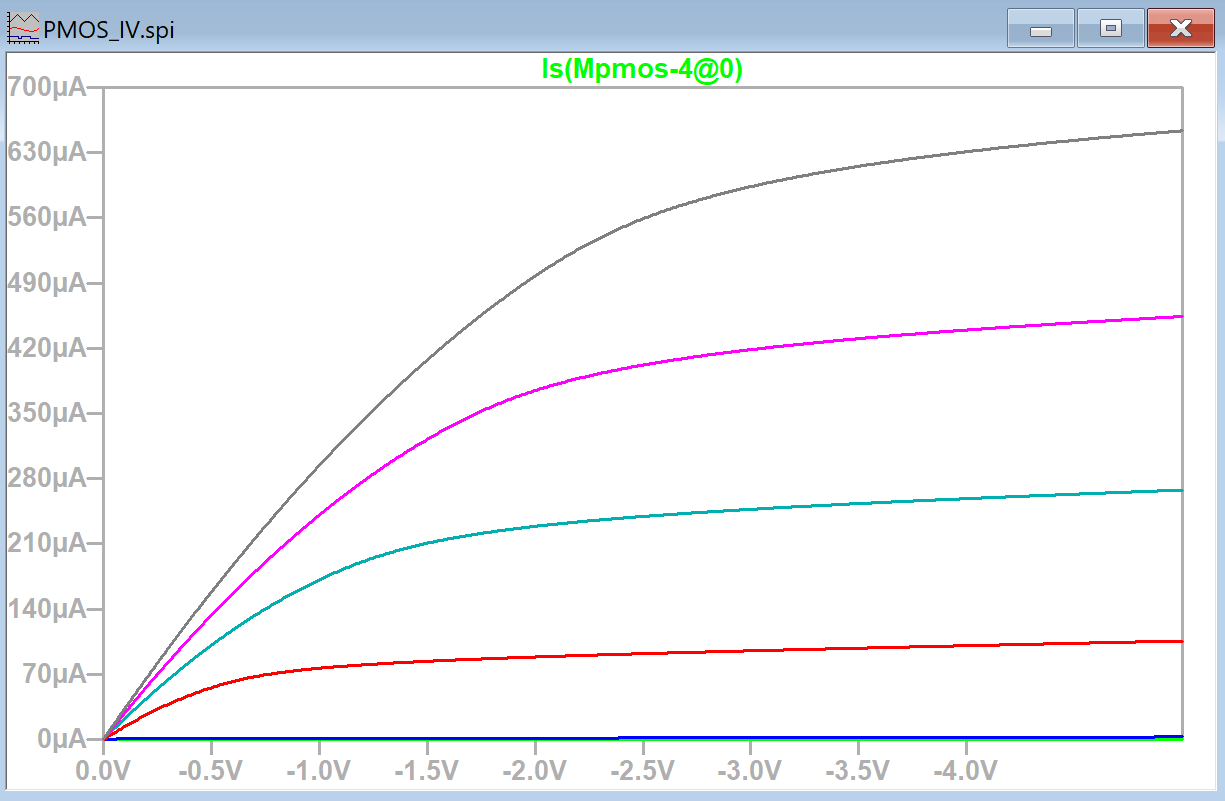
Figure 40.The
LTSpice simulation plot for the final PMOS IV schematic.
Discussion
I
thought this lab provided a good information on how the layout works
and it showed how the schematic needs to match the layout view with the
width and exported pins. It also showed how connections like the p-well
layer for the NMOS IV work and that by just overlapping nodes can make
that connection. When following the tutorial I found that my Electric
VLSI didn't behave like the tutorial's version of Electric VLSI. If you
look at Figure 8 and Figure 22, the same connection was made but my
connection didn't need to be modified at all. I could directly repeat
the steps for the first N-Active Arc connection and my layout view
still passed the relevant checks. I'm not sure why this happened, I
even looked into the Arc's properties and nothing made it behave like
in the tutorial. I also ran into another issue with the NMOS IV
schematic. It wasn't immediately clear to me that the NMOS IV schematic
should be changed to a 4-port transistor like the PMOS IV schematic so
I continued the tutorial never changing that as seen in Figure 35. I
did add the change to connect the ground symbol in the schematic but
then I ran into another issue. My simulation plot for the NMOS IV
schematic did not match the plot for the NMOS IV layout even though I
connected everything appropriately. This is seen in Figures 34 and 38.
I think it may have something to do with the ground pin but my
schematic does match the tutorial's schematic. Those were the only
issues I ran into with this lab however.