ENGR338 Lab 2021
Spring
Lab 3 Layout the R-2R DAC
Name: Sean
Eaton
Email:
smeaton@fortlewis.edu
Layout the R-2R DAC
Introduction
In this
lab we will be creating subcells out of the repeating structure found
in the R-2R ladder DAC we designed in Lab 2. Using the subcells the
R-2R ladder will be reimplemented as R_2R_Ladder_V2 and an icon view
will be created for it. Next a layout view will be created that uses
N-well resistors. After this is done we will verify that the simulation
behaves as expected with the ideal ADC to R-2R ladder DAC V2 schematic.
Task 1: Create the schematic of the subcells for the R-2R ladder.
A new schematic called 'R_2R_Subcell' should be created that should look like the one shown below in Figure 1.
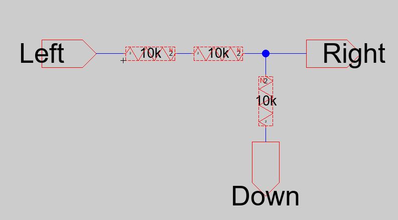
Figure 1. R_2R_Subcell schematic.
The subcell looks like that because the R-2R ladder has a repeating structure in it as shown below in Figure 2.
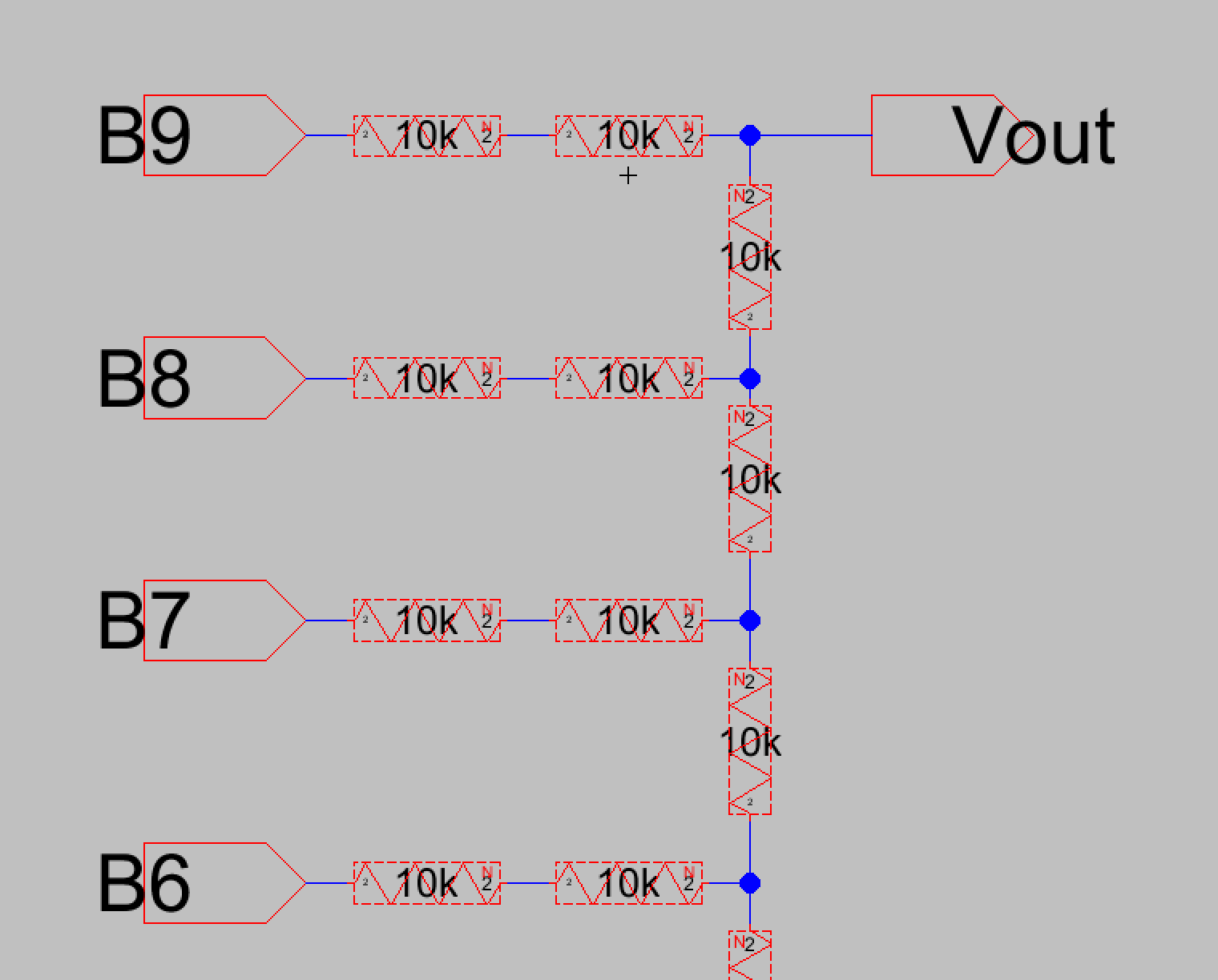
Figure 2. Repeating structure in the R-2R ladder DAC.
Next an icon should be created for the subcell as shown below. A DRC Check should also be performed at this point.
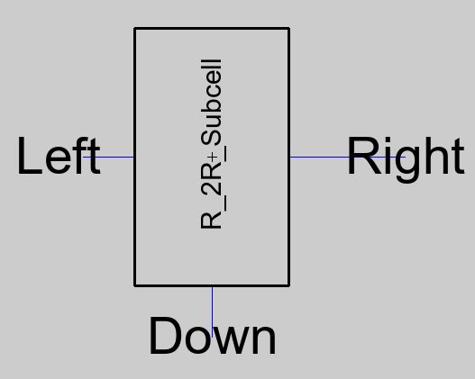
Figure 3. R-2R Subcell icon.
Use
the subcell icon to create the R_2R_Ladder_V2 schematic as shown below.
Make sure that the subcell for B0 has an added 10k ohm resistor
connected to ground just like the R-2R ladder designed in Lab 2. After
this another DRC Check should be run.
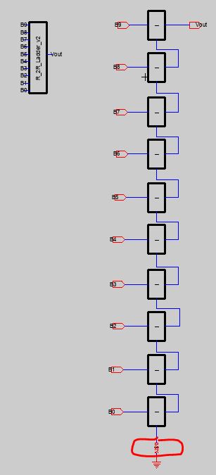
Figure 4. R_2R_Ladder_V2 schematic.
Task 2: Create the layout of the subcells for the R-2R ladder.
To
create the layout for the R_2R_DAC_V2 schematic, the layout for the
R_2R_Subcell should first be created. In order to get a 10k ohm
resistor the properties of the "N-RWell" component should be edited. A
width of 15 and length of 187.5 is required since the sheet resistance
of an n-well is about 800 ohms in the C5 process.
187.5 / 15 = 12.5 squares
12.5 squares * 800 ohms/square = 10k ohms
The
layout for the R_2R_Subcell will need to match the subcell schematic
created in task 1, so three 10k ohm n-well resistors need to be laid
out like so. The spacing in between n-wells is 25. After completing the
layout a DRC Check should be ran as well as NCC.
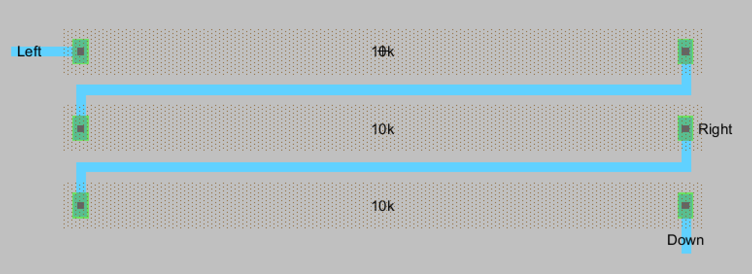
Figure 5. R_2R_Subcell layout view.
To
create the layout for the R_2R_Ladder_V2 use the layout of the
R_2R_Subcell. The subcell layout should be centered first and then the
Edit > Array function can be used to create 10 copies of the layout.
When
using the Array function, input 10 for the "Y repeat factor", select
"Space by centerline distance", input 214.25 for "X centerline
distance", and 75 for "Y centerline distance" as shown below in Figure
6.
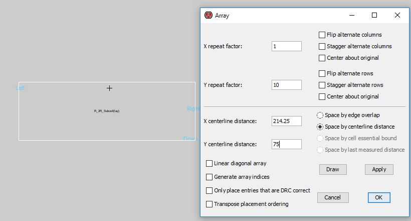
Figure 6. Using the Array function to create ten copies of the subcell layout.
After
creating the ten copies run another DRC check to ensure there aren't
any errors before wiring. Also, make sure an additional 10k ohm n-well
resistor is added at the bottom, just like in the schematic. When wiring is completed, run another DRC and NCC check as shown below.
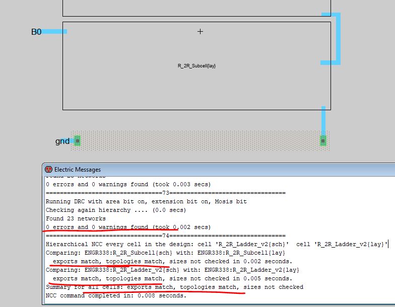
Figure 7. The layout view with the added 10k ohm n-well resistor in addition to DRC and NCC results.
Now
the R_2R_Ladder_V2 icon can be added to a simulation schematic. The
simulation schematic is the same ideal ADC to ideal DAC one used in Lab
2. Just replace the ideal DAC with the new R_2R_Ladder_V2 icon and
verify the LTSpice simulation is similar to the results found in Lab 2
as shown below in Figure 8.
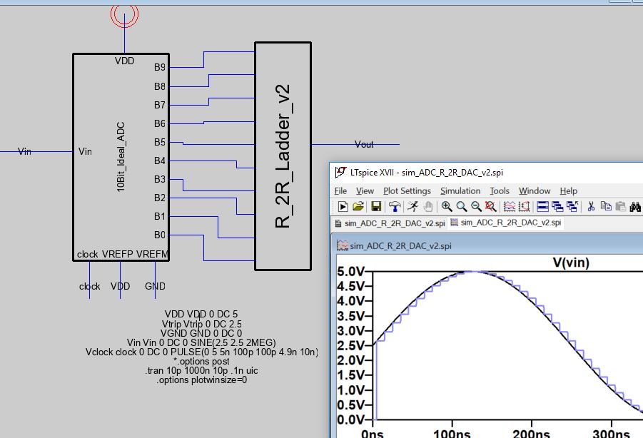
Figure 8. Simulation schematic and LTSpice simulation plot for the R_2R_Ladder_V2.
Results
Task 1:
The
schematic and icon for the R-2R ladder subcell was successfully
created. It also passed the DRC check as shown below in Figure 9.
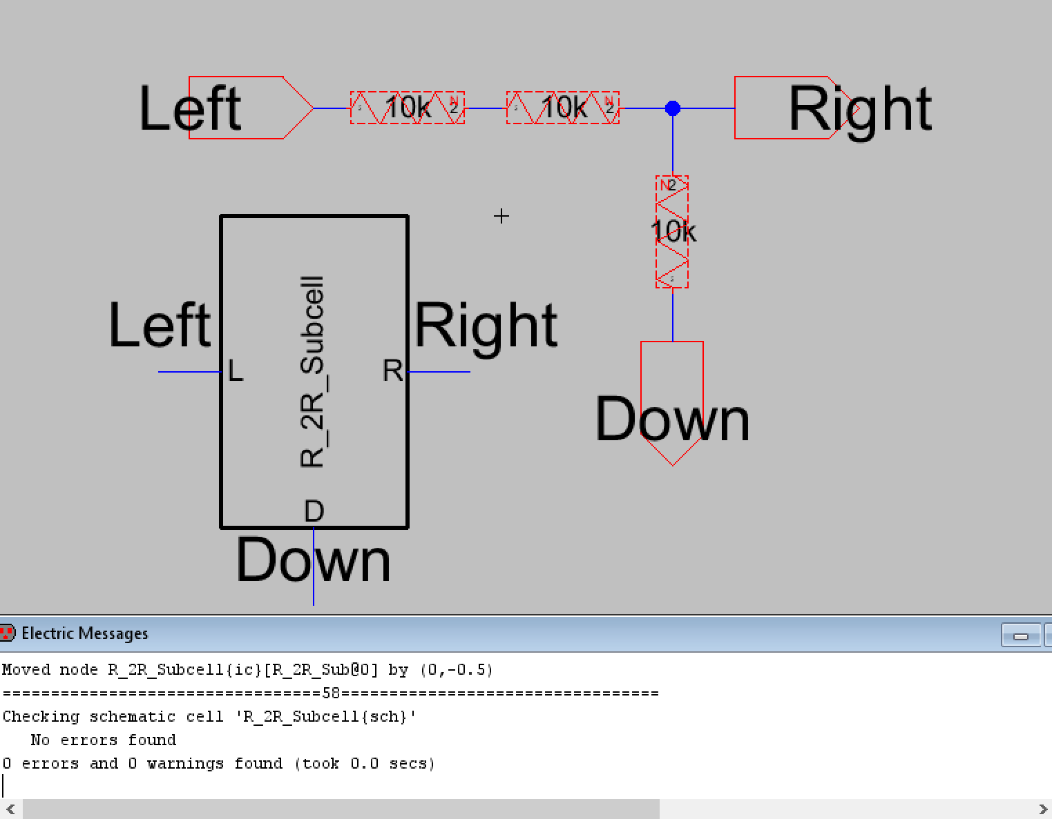
Figure 9. Screenshot of the R-2R Ladder subcell schematic, its icon and DRC results.
Using
the subcell, the R-2R ladder V2 schematic was created. The bottom
subcell has a 10k ohm resistor connected to ground added and the DRC
check passed with no errors or warnings.
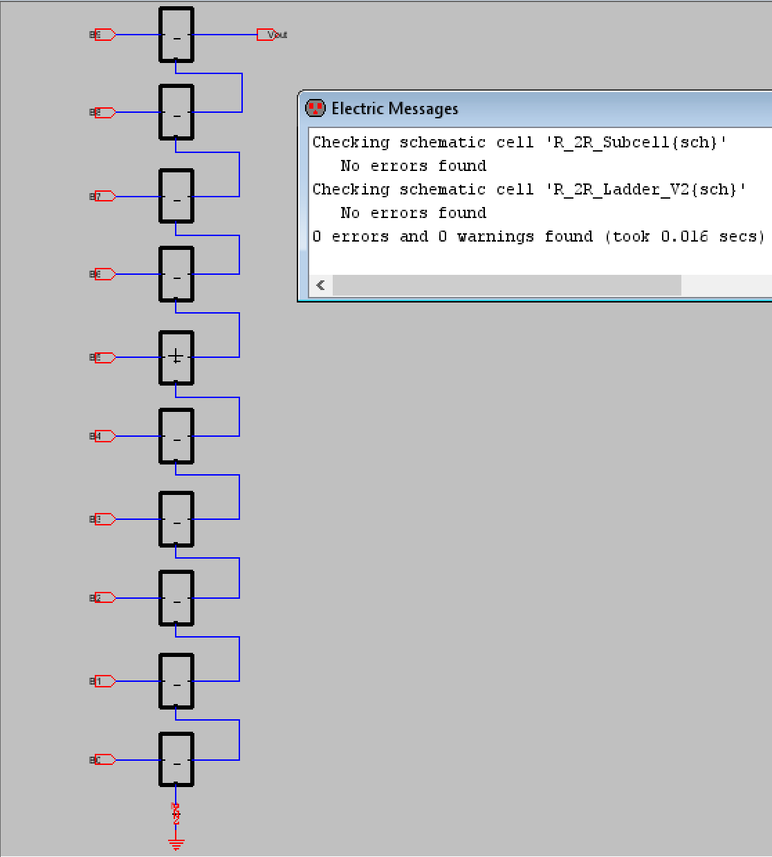
Figure 10. The R-2R ladder V2 schematic with its DRC results.
The
icon for the R-2R ladder V2 was also created. Figure 11 show the icon
in addition to a closer look at the subcells and the additional DRC
check.
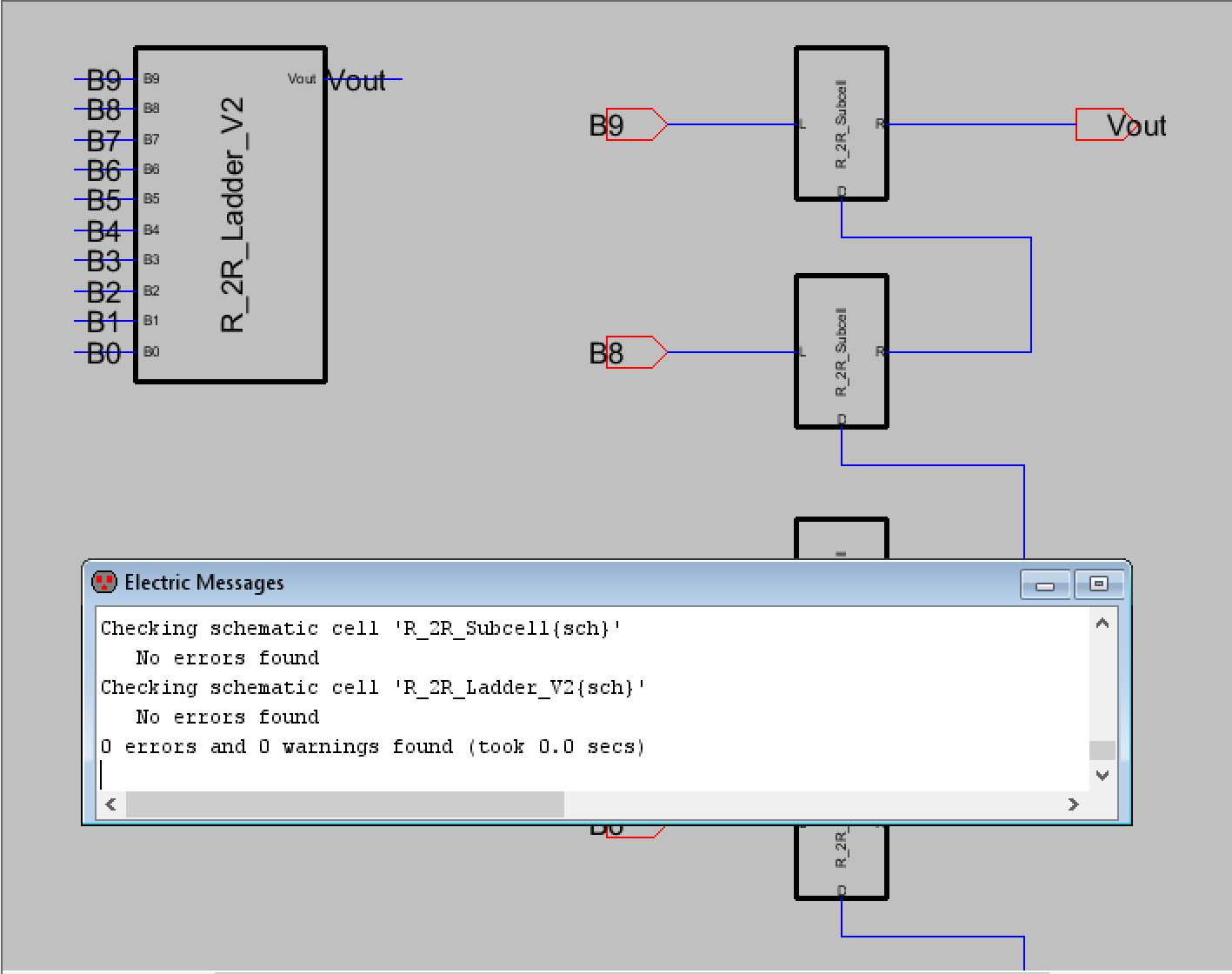
Figure 11. A closer look at the R-2R ladder V2's schematic, icon, and successful DRC check.
Task 2:
The
appropriate n-well resistors were set up and used to create the layout
view for the R-2R subcell and the DRC check passed without any issues
as shown below in Figure 12.
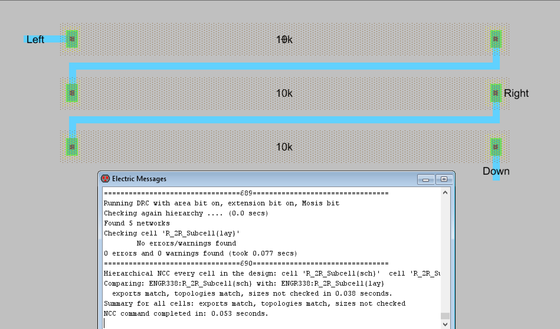
Figure 12. The layout view for the R-2R subcell with the DRC check results.
Next
the layout view for the R-2R ladder V2 was created. The R-2R subcell
layout was also used for this and 10 copies were created using the
Array function. Beofre any wiring was done another DRC check was ran
which it passed as shown below.
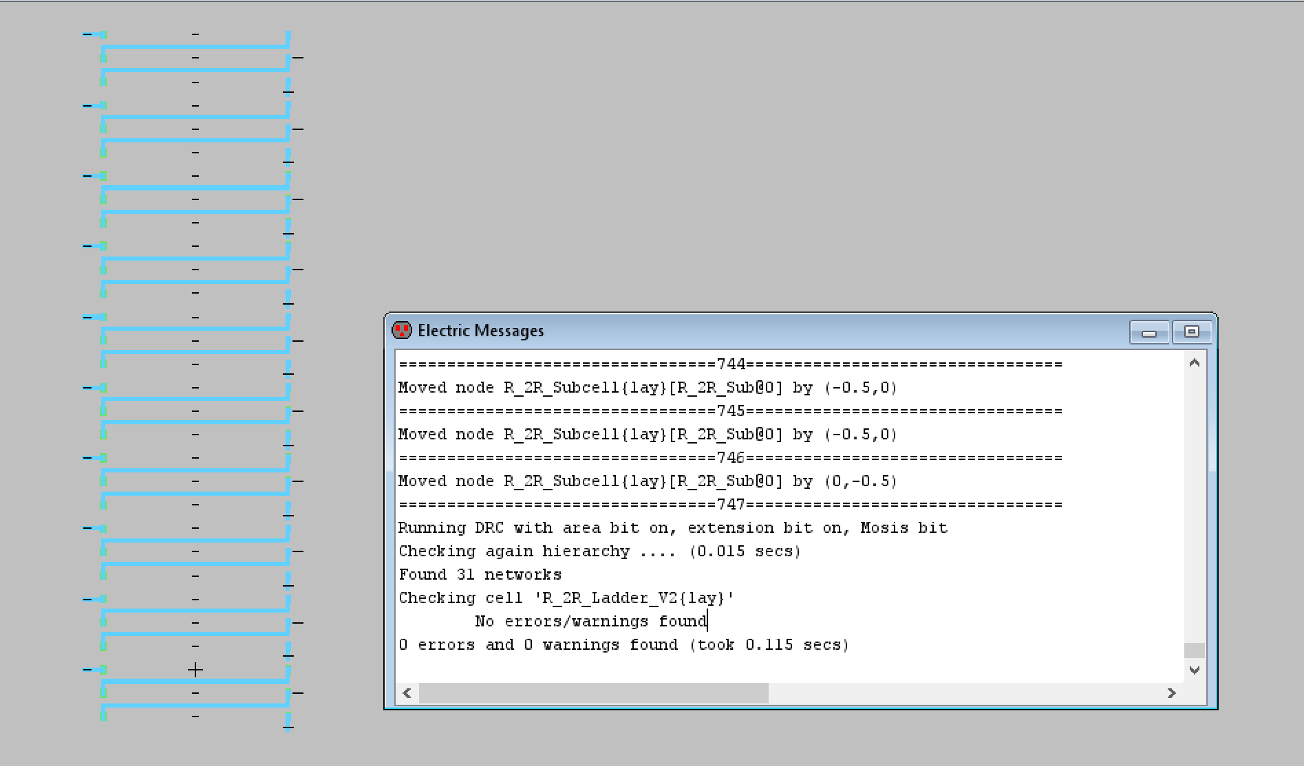
Figure 13. R-2R Ladder layout view passes DRC check prior to wiring.
Now
that the layout view passed the DRC check everything was wired together
appropriately, pins for the digital inputs, vout, and gnd were
exported, and an additional 10k ohm n-well resistor was placed at the
bottom. This is shown in Figure 14 as well as the successful DRC and
NCC checks.
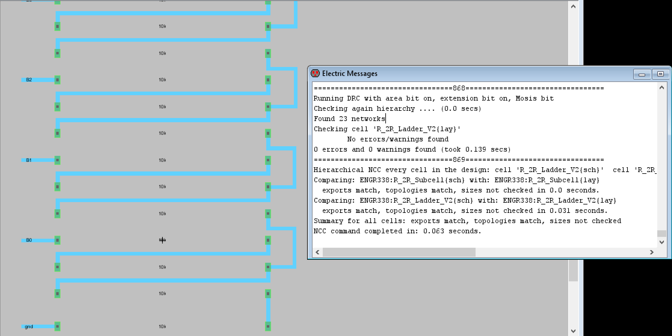
Figure 14. The finished layout view for the R-2R Ladder V2. The added 10k ohm n-well resistor is shown at the bottom as well.
The
simulation schematic for the ideal ADC to ideal DAC was copied and
edited so that it used the ideal ADC to the R-2R Ladder V2 icon created
in Task 1. The LTSpice simulation was run and the results were as
expected. Figure 15 shows the simulation schematic used and Figure 16
shows the results of the LTSpice simulation with Vin and Vout plotted.
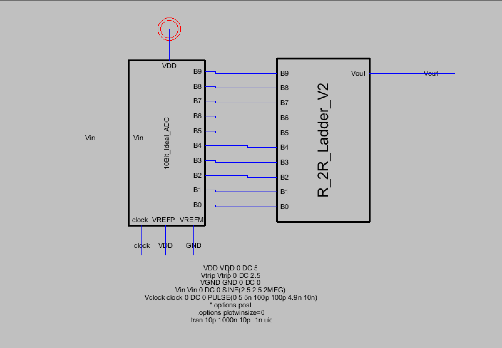
Figure 15. The simulation schematic for the ideal ADC to R-2R Ladder V2 icon.
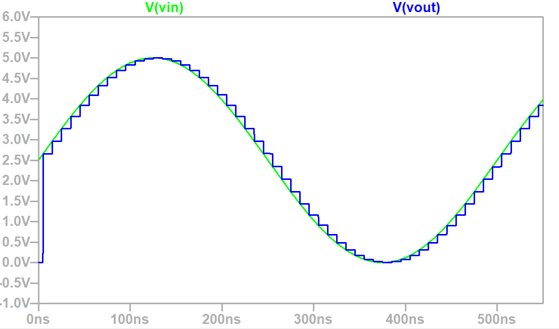
Figure 16. LTSpice simulation plot of Vin compared to Vout.
Discussion
This lab provided me with more experience using Electric VLSI and it
showed me how creating a layout view works. Creating the R-2R ladder
using subcells was also more convienent than the previous method in Lab
2 since the subcell could be used for creating other R-2R ladders such
as an 8-bit input one.